Science 'Touching' the Surface of an Atom: The Architecture and Methodology of Scanning Probe Microscopy
An in-depth understanding of the science and complex structure of microscopes that create atomic-level images by probing surfaces with an extremely fine needle instead of light rays.

In human history, the advancement of science has always been intertwined with our capacity to see. When we built optical microscopes to observe cells, it revolutionized biology. But when it came to viewing matter at the atomic scale, rays of light fell short. To break this limitation, in 1981 IBM scientists Gerd Binnig and Heinrich Rohrer developed a technology that does not see, but rather 'touches'. This technology is Scanning Probe Microscopy (SPM). This discovery was so epoch-making that it earned them the Nobel Prize in Physics in 1986.
Scanning Probe Microscopy is a family of microscopes that uses a physical probe, namely an extremely fine needle, to image surfaces. This probe scans the surface and collects data based on it. Traditional microscopes use lenses and light rays, which cannot see beyond a certain level of detail due to the diffraction limit—that is, the limitation of light waves. SPM overcomes this limitation because it does not depend on light. Its resolution capacity is so remarkable that it can capture details down to a tenth of a nanometer.
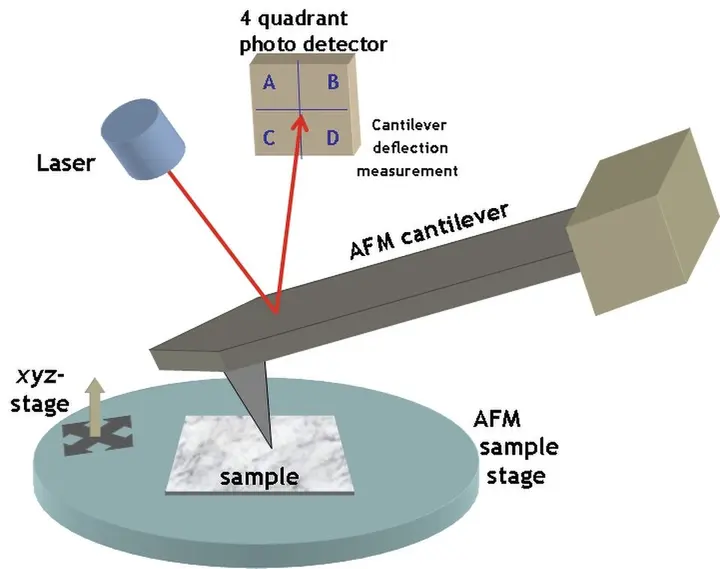
The core secret behind the working mechanism of this microscope is piezoelectric actuators. These are devices capable of making extremely minute movements upon receiving an electric signal. This movement can be even smaller than the size of an atom. With the help of these actuators, the probe is moved across the surface with extreme precision in the x, y, and z directions. This entire process is called a raster scan, in which the probe moves across the surface line by line and records data at each point.
- Piezoelectric actuatorsThe probe is moved with extreme precision in X, Y and Z directions by electrical signals.
- Raster scanThe probe moves line by line across the surface, recording data at each point.
- Effect of forcesThe cantilever bends or deflects due to forces between the probe and surface atoms.
- Feedback loopThe system constantly moves the probe up and down to keep the distance between the probe and surface constant.
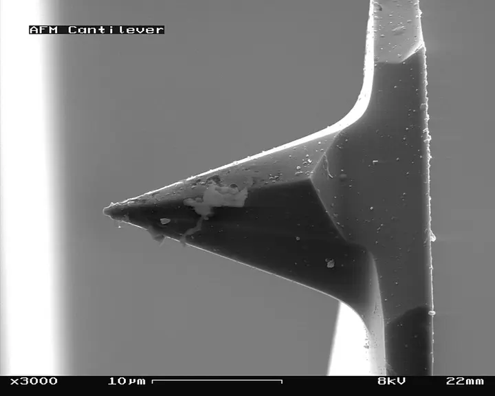
The best-known name in the SPM family is Atomic Force Microscopy (AFM). The structure of AFM features a cantilever, which looks like a diving board in appearance. At the end of this cantilever is an extremely sharp tip or needle. When this tip comes close to a surface, various forces begin to act between the atoms of the tip and the surface. These forces include van der Waals forces, capillary forces, and electrostatic forces. Due to these forces, the cantilever bends or deflects.
- Bringing the probe closeThe extremely fine tip is brought so close to the surface that atomic forces become active.
- Raster scanningThe probe is moved in an X-Y grid across the surface with the help of piezoelectric actuators.
- Deflection measurementThe cantilever bends according to surface fluctuations, which is recorded by the laser and photo detector.
- Feedback controlThe feedback loop maintains a constant distance and records these changes as data.
- Image generationComputer software processes this data to create a 3D map of the surface.
A laser system is used to measure this deflection. A laser beam is directed at the back surface of the cantilever, which is reflected and falls on a photo detector. If the cantilever bends even slightly, the position of the laser beam on the detector changes. This change is so minute that it can be converted into an electrical signal and a computer can generate a surface map. In this way, the AFM 'feels' the surface to create its 3D topography, meaning the structure of the surface.
A feedback loop is extremely important for the functionality of an SPM. A feedback loop is a system that continuously maintains the distance between the probe and the surface. Generally, a PI-loop is used for this. When the probe encounters a raised part on the surface, the feedback system immediately lifts the probe slightly so that it does not collide with the surface. In this way, the force or distance between the probe and the surface is kept constant. The height of the surface is determined precisely on the basis of the voltage that must be applied to move the probe up and down.
The resolution capacity of the microscope depends on how sharp the tip of the probe is. Ideally, if we want atomic-level resolution, there should be only a single atom at the end of the tip. This tip is generally made of silicon or silicon nitride. In instruments like the Scanning Tunneling Microscope (STM), platinum-iridium or tungsten wire is used. This wire is cut or electrochemically etched in such a way that its end becomes extremely sharp. If the tip is blunt or has more than one point at its end, flaws can appear in the image, which are called ghost images.
SPM has mainly two operating modes: constant interaction mode and constant height mode. In constant interaction mode, the feedback loop is active and moves the probe up and down according to the undulations of the surface. This mode is safe because the probability of the probe colliding with the surface is lower in it. On the other hand, in constant height mode, the probe is scanned while kept at a single height. Scanning can be done quickly in this mode, but if a sudden raised part appears on the surface, there is a risk of the probe breaking. Therefore, it is necessary to check how flat the surface is before using this mode.
There are three sub-modes in AFM as well: contact mode, tapping mode, and non-contact mode. In contact mode, the tip continuously touches the surface. In tapping mode, the cantilever is oscillated at a specific frequency so that the tip moves as if gently tapping the surface. This method is best for soft materials or biological samples because it does not damage the surface. In non-contact mode, the tip stays slightly away from the surface and acquires data based solely on atomic forces.
| Type | Medium of measurement | Sample requirement |
|---|---|---|
| STM | Tunneling current (electric) | Conductive surface only |
| AFM | Atomic force (mechanical) | Any surface |
| MFM | Magnetic force | Magnetic materials |
| KPFM | Electric potential | Conductive or semiconductor |
Speaking of the advantages of SPM, it not only creates an image of the surface but can also measure material properties. For instance, magnetic fields on the surface can be observed through Magnetic Force Microscopy (MFM), while the electrical conductivity of the surface can be measured via Conductive AFM (C-AFM). In addition, atoms can be moved from one place to another using this microscope, which is called atomic manipulation. This capability is foundational for creating new devices in nanotechnology.


However, SPM also has certain limitations. The process of acquiring images with this method is quite slow because the probe has to physically move across the entire surface. Furthermore, the scanning area is also quite small, typically less than 100 micrometers. Errors in measurement can also occur due to thermal drift over time, which is the microscopic expansion caused by temperature changes. This is why ultra-low temperature and vacuum conditions are required for extremely precise experiments.
In modern science, SPM is widely used in the semiconductor industry, battery research, and biology. AFM is also being used to measure the difference in hardness between cancer cells and normal cells. In India as well, IITs and other research institutes utilize this technology for the study of nanomaterials. As software and algorithms continue to improve, the analysis of data obtained through this microscope becomes more accurate, helping us unlock new secrets of the invisible world of atoms.