Hardware That Evolves Like Software: The FPGA Architecture Revolution in the AI Era
Capable of being reprogrammed even after factory production, FPGA chips are accelerating artificial intelligence and data center workloads.

In the world of computing processing, there are generally two types of chips: a Central Processing Unit (CPU), which can perform any task according to software instructions but has limited speed, and an Application-Specific Integrated Circuit (ASIC), which is permanently built onto silicon in a factory for only one specific task. However, an extremely powerful option exists between these two, which is called a Field-Programmable Gate Array (FPGA).
An FPGA is a configurable integrated circuit that can be repeatedly programmed by the user even after it has been manufactured and left the factory. It is placed in the class of Programmable Logic Devices (PLD). This chip contains a mesh grid of programmable logic blocks, which can be configured in the field to perform various digital tasks by connecting them with other logic blocks.
According to company announcements, the importance of FPGAs has grown unprecedentedly in the fields of Artificial Intelligence (AI) and high-performance computing. Microsoft began using FPGAs in 2014 to accelerate its Bing search engine, and in 2018, it started deploying FPGA chips for various workloads on its Azure cloud computing platform. The main reason for this is the excellent performance per watt efficiency provided by FPGAs. Since 2019, special AI engines have been added to modern-generation FPGAs to process artificial intelligence models.
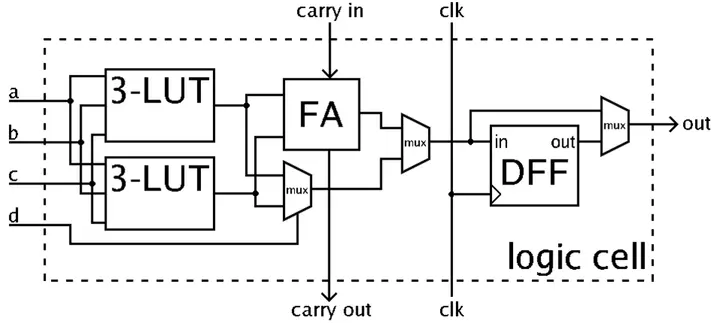
- Look-Up Table (LUT) processingInput signal enters 4-input LUT where logical result is prepared according to pre-defined truth table.
- Mode selection and multiplexingProgrammed multiplexer determines whether the cell will work in normal logic mode or arithmetic calculation mode.
- Full adder calculationIn arithmetic mode, the output of the LUT is sent to a Full Adder for fast calculation of sum and carry.
- Synchronization and outputThe result is stored synchronously in a D-type flip-flop or sent asynchronously to the internal routing network.
The history and evolutionary journey of FPGAs
The history of FPGAs began with Programmable Read-Only Memory (PROM) and Programmable Logic Devices (PLD). In both these technologies, the option to program the chip at the factory or at the user's site was available.
The first major step in this field was taken by the company Altera in 1984, following its founding in 1983. They introduced the industry's first reprogrammable logic device, the EP300. This chip featured a quartz window on its packaging, through which the chip configuration stored in the EPROM cell could be erased by shining light from an ultraviolet (UV) lamp.
Subsequently, in 1985, the company Xilinx (now acquired by AMD) introduced the first commercially successful FPGA chip, the XC2064. This chip featured programmable gates and programmable interconnects between the gates. The XC2064 included 64 Configurable Logic Blocks (CLBs) and two 3-input Lookup Tables (LUTs).
In 1987, the Naval Surface Warfare Center funded an experiment proposed by Steve Casselman, which aimed to build a computer containing 600,000 reprogrammable gates. Casselman succeeded in this experiment, and a patent for this system was obtained in 1992.
By 1993, the company Actel had captured approximately 18% of the market. According to 2013 data, Altera (31%), Xilinx (36%), and Actel (10%) together held approximately 77% of the global FPGA market. The gate capacity of FPGAs increased from 9,000 gates in Xilinx in 1987 to 50 million gates in 2013.
In financial terms, this market was worth $14 million in 1987, which grew to over $385 million in 1993. It reached $1.9 billion in 2005, $2.75 billion in 2010, and $5.4 billion in 2013. The market was estimated to reach $9.8 billion in 2020 and is projected to grow to $23.34 billion by 2030. The number of new FPGA design starts was 80,000 in 2005, which increased to 90,000 in 2008.
બિલિયન ડૉલર
Internal Architecture: Design of Logic Cells and LUTs
The basic architecture of an FPGA consists of a grid of Configurable Logic Blocks (CLBs) or Logic Array Blocks (LABs), input/output pads (I/O pads), and routing channels. Generally, all routing channels have the same width or signal capacity.
A typical logic cell is composed of three main components: a 4-input Look-Up Table (4-input LUT), a Full Adder (FA), and a D-type flip-flop. The 4-input LUT can be divided into two 3-input LUTs. In normal mode, these two are combined via a first multiplexer (mux) to form a 4-input LUT. In arithmetic mode, their outputs are sent to an adder. The mode selection is performed by a second multiplexer, while the output can be obtained in synchronous or asynchronous mode with the help of a third multiplexer via programming.
The requirement for routing channels for any design depends on the type of circuit. For example, a crossbar switch requires more routing than a systolic array. Unused routing channels increase costs and reduce performance, so manufacturers provide an appropriate number of channels based on 'Rent's rule' estimates.
| Year / Model | Manufacturer Company | Main architectural detail | Special feature |
|---|---|---|---|
| 1984 (EP300) | Altera | First reprogrammable logic | UV quartz window for EPROM erasing |
| 1985 (XC2064) | Xilinx | 64 CLBs, two 3-input LUTs | First commercial FPGA chip |
| 2012 (Zynq-7000) | Xilinx | 1.0 GHz dual-core ARM Cortex-A9 | All-programmable SoC integration |
| 2012 (Arria V) | Altera | 800 MHz dual-core ARM Cortex-A9 | System-on-chip architecture |
Hard Blocks, Soft Cores, and System-on-Chip Integration
Modern FPGAs are not limited to just logic gates. They incorporate high-level functionality circuits etched onto silicon as permanent hardware, known as 'hard blocks'. These include silicon multipliers, DSP blocks, embedded memory, and high-speed transceivers. Since these hard IP cores are built directly from transistors, they provide high efficiency and low power consumption comparable to ASICs.
The second approach is the 'soft processor core', in which a processor is built using the FPGA's programmable logic. Nios II, MicroBlaze, and Mico32 are popular soft-core processors of this type.
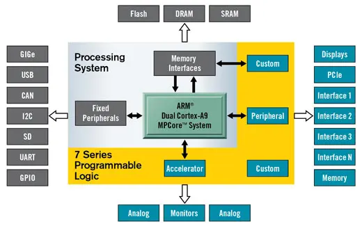
In 2012, the technology industry took a new turn when FPGA logic and internal interconnects were combined with an embedded microprocessor to create a System on Chip (SoC) on a programmable chip. The Xilinx Zynq-7000 All-Programmable SoC is an excellent example of this, in which a 1.0 GHz dual-core ARM Cortex-A9 MPCore processor was integrated into the FPGA's logic fabric. Similarly, the Altera Arria V FPGA featured an 800 MHz dual-core ARM Cortex-A9 processor. The Microsemi SmartFusion device was equipped with an ARM Cortex-M3 processor along with 512 kB of flash and 64 kB of RAM.
The Importance of Clocking, Signaling, and Testing
Most of the internal circuitry of an FPGA is synchronous, requiring a clock signal. To ensure there is no skew in the signal, FPGAs utilize special H-tree shaped global and regional routing networks. Additionally, analog Phase-Locked Loops (PLL) and Delay-Locked Loops (DLL) are used for frequency synthesis and jitter management.
High-speed serializer and deserializer (SERDES) circuits are used to transfer data outside the chip. The configuration code for an FPGA is typically written in a Hardware Description Language (HDL) such as VHDL. This technology is used extensively in the automotive, aerospace, and telecom sectors, as well as to accelerate the simulation process before manufacturing an ASIC chip.