The Data Revolution: The Inner Workings of SSD and NAND Flash Memory Architecture
From mechanical hard disks to modern 3D NAND and 3D XPoint technologies: How do SSDs function and how has flash memory transformed the world of computing?

If there is one technological shift in the field of data storage for computers and mobile devices that stands out over the last two decades, it is the rise of the Solid-State Drive (SSD). Traditional Hard Disk Drives (HDD) utilized mechanical parts such as spinning magnetic disks and moving heads to read and write data. In contrast, an SSD operates entirely on solid-state storage technology. It contains no moving mechanical parts, but instead uses semiconductor integrated circuits for storage.
SSDs primarily use non-volatile memory (memory that retains data even when power is cut off) for data storage, which is commonly known as NAND flash memory. Due to the absence of mechanical parts, SSDs offer faster data access speeds, extremely low latency (the time taken to retrieve data), high resistance to physical shock, lower power consumption, and completely silent operation. According to a Wikipedia report, the performance and durability of an SSD depend on how many bits are stored per memory cell.
The History of Flash Memory: From EEPROM to NAND
The origins of flash memory lie in the invention of the Floating-Gate MOSFET (FGMOS). Following the invention of the original MOSFET at Bell Labs between 1959 and 1960, Dawon Kahng and Simon Min Sze proposed the floating-gate transistor in 1967. While EPROM and EEPROM were developed from this technology in the 1970s, it was an extremely expensive and slow solution at the time because a separate cell had to be created for each bit.
Modern flash memory was invented in 1980 by Fujio Masuoka, a scientist working at Toshiba. According to a Toshiba report, because the data erasure process was as quick as a camera flash, Masuoka's colleague Shoji Ariizumi suggested naming it "flash." Masuoka and his team introduced the concept of NOR flash in 1984 and subsequently NAND flash memory at the IEEE IEDM conference held in San Francisco in 1987. Toshiba launched the first commercial NAND flash in 1987, while Intel brought the first NOR flash chip to market in 1988.
NOR flash memory facilitates byte-level random access, which is suitable for running a computer's BIOS or program code. However, in NAND flash memory, data is written and erased in the form of blocks or pages. NAND flash occupies less space on a chip and the production cost per bit is much lower, making it the ideal technology for mass storage devices like SSDs and memory cards.
- 1. Data WritingNew data coming from the host computer is written into empty pages of NAND flash memory.
- 2. Data ModificationWhen existing data is modified, the new data is written to a new page and the old data is marked as invalid.
- 3. Garbage CollectionThe controller separates valid data from blocks containing invalid data in the background and transfers it to a new block.
- 4. Block ErasingThe entire block containing only invalid data is erased at once and cleared for future write operations.
Internal Architecture of an SSD and the Role of the Controller
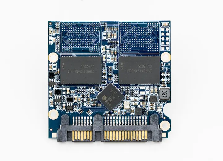
Any SSD has two main components: the controller and the NAND flash memory chips. The controller is the brain of the SSD; it is an embedded processor running specialized firmware. It manages all data flow between the host computer and the NAND memory.
The controller performs several complex tasks simultaneously. These include bad block mapping (removing defective cells), read/write caching, data encryption, error correction via ECC (Error-Correcting Code) such as BCH codes, and overall thermal management. Furthermore, garbage collection (clearing unused data) and wear leveling are extremely important in an SSD. Repeatedly writing data to NAND cells causes them to wear out, so wear leveling algorithms extend the lifespan of the SSD by distributing data evenly across all chips.
| Cell Type | Bits per Cell | Performance and Lifespan | Main Use / History |
|---|---|---|---|
| SLC (Single-Level Cell) | 1 bit | Highest speed and maximum lifespan | Enterprise Data Center |
| MLC (Multi-Level Cell) | 2 bits | High performance and long lifespan | Professional SSDs (NEC 1998) |
| TLC (Triple-Level Cell) | 3 bits | Balanced speed and reasonable price | General Consumer SSDs (Samsung 2010) |
| QLC (Quad-Level Cell) | 4 bits | Slower speed, lower lifespan, minimum cost | High-capacity affordable storage (2009) |
Due to the internal parallelism embedded in an SSD, when the controller works across multiple NAND channels simultaneously, data transfer bandwidth increases and latency is significantly reduced.
Types of Memory Cells: SLC, MLC, TLC, and QLC
The storage capacity of a NAND flash memory cell depends on its architecture. Fundamentally, a Single-Level Cell (SLC) stores only 1 bit of data per cell. SLC drives offer the highest processing speed and the longest lifespan, but they are extremely expensive.
As technology advanced, Multi-Level Cell (MLC: 2 bits per cell), Triple-Level Cell (TLC: 3 bits per cell), and Quad-Level Cell (QLC: 4 bits per cell) were developed. Commercial production of 2-bit MLC was started by NEC in 1998, and TLC by Samsung in 2010. In 2009, Toshiba and SanDisk introduced QLC technology with a capacity of 64 Gb. Storing more bits per cell increases storage capacity and reduces cost, but it decreases the cell's lifespan and write speed.
In addition to this, 3D XPoint technology (such as Intel Optane), developed by Intel and Micron, stores data by changing electrical resistance instead of storing an electric charge in a memory cell. This method provides significantly higher speed and longer lifespan than traditional flash memory.
The Revolutionary Mathematics of Charge Trap Flash and 3D NAND
As the physical limitations of shrinking silicon transistor sizes were reached, the semiconductor industry adopted Charge Trap Flash (CTF) technology. CTF uses an insulating layer of silicon nitride instead of a traditional polysilicon floating gate to trap electrons. Researchers at NEC demonstrated this method in 1991, and it was commercially launched by AMD and Fujitsu in 2002.
લેયર્સ (Layers)
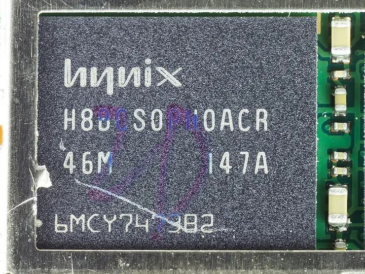
Instead of building chips only on a flat (2D) surface, 3D V-NAND (Vertical NAND) technology was created by stacking cells on top of each other. Toshiba introduced an 8-layer chip package (THGAM0G7D8DBAI6) under 3D IC technology in 2007, and SK Hynix demonstrated 24-layer 3D IC technology. In 2013, Samsung began production of the first commercial 24-layer 3D V-NAND chip, which caused an explosive increase in the storage capacity of modern SSDs.
Standards for SSD Lifespan and Reliability
Specific metrics have been defined by the JEDEC organization to determine the durability of an SSD. These include Terabytes Written (TBW), Drive Writes Per Day (DWPD), and Unrecoverable Bit Error Ratio (UBER). The lifespan of a flash cell primarily depends on the number of its program-erase cycles (P/E cycles).
For example, the Samsung 970 EVO NVMe M.2 SSD (2018) with a capacity of 1 TB has an endurance rating of 600 TBW. This means that over its lifetime, a user can write 600 terabytes of data, which is equivalent to approximately 600 P/E cycles. Since there are no mechanical parts, SSDs are resistant to shocks, but there is a risk of data loss due to gradual charge leakage if consumer-grade SSDs are left in storage without power for a long time (1 to 2 years).
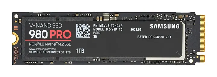
Starting from the original SATA and mSATA interfaces, today's SSDs operate on advanced M.2, PCIe, and NVM Express (NVMe) protocols. The NVMe architecture supports high-speed parallel queues, which allows for maximum utilization of the computing system's bus lines. Continuous research is underway to make SSD technology faster and denser for future data center and AI workloads.