The Heart of the Semiconductor Revolution: An In-depth Look at Silicon Wafers and the Complex Process of Photolithography
How are modern chips made? A scientific journey from sand to silicon wafers, and the process of etching billions of circuits using light.
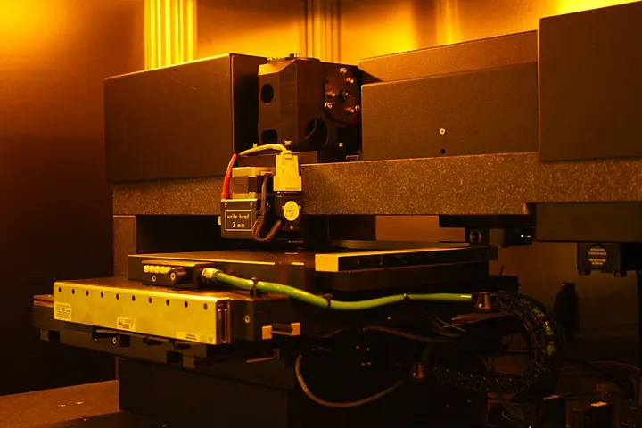
In the world of modern technology, the smartphones, laptops, and artificial intelligence we use are powered by semiconductor chips. The process of manufacturing these chips is extremely complex and demands high precision. There are two main aspects to this process: one is the silicon wafer, which acts as a canvas for the chip, and the other is photolithography, which works to etch billions of circuits onto this canvas. These two processes are like two sides of a coin, which can be called a 'Janus-faced' process, as it is a remarkable confluence of materials science and optical engineering.
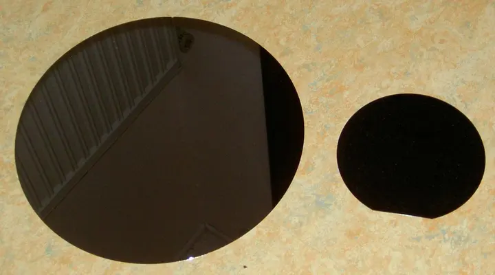
The term 'wafer' became prevalent in the semiconductor industry in the 1950s. According to a Wikipedia report, a wafer is an extremely thin, circular slice of semiconductor material. It is typically made from crystalline silicon. It is on these wafers that microelectronic devices are built, which subsequently become parts of our gadgets. The wafer manufacturing process begins with sand and must be extremely pure.
The 'Czochralski method' is the most well-known technique for wafer production. In this method, highly purified silicon is melted, and a cylindrical crystal (boule) is pulled from it. The purity of this crystal is even greater than 99.9999999% (9N). This cylinder is then cut into thin slices using a wire saw, which we call wafers. To make the surface of these wafers extremely flat, they are polished with chemicals.
- Cleaning and preparationThe wafer is chemically cleaned and heated to 150 °C to remove moisture.
- Photoresist applicationA thin layer of light-sensitive photoresist is applied to the wafer by spin coating.
- ExposureIntense light is projected onto the wafer through a photomask, so the circuit design is imprinted on the photoresist.
- DevelopingExcess photoresist is removed using a special solution so that the pattern appears on the wafer.
The size of a wafer has a major impact on its production cost and efficiency. In the early days, wafers were only 1 inch in size, but today 300 mm (11.8 inches) wafers are standard. Companies like Intel and Samsung are also researching 450 mm wafers. The advantage of larger wafers is that more chips can be made on them simultaneously, which reduces the cost per chip. However, the machinery cost to produce 450 mm wafers can increase by 20% to 50%, which is a significant challenge.
| Material | Maximum commercial size | Status |
|---|---|---|
| Silicon (Si) | 300 mm | In widespread use |
| Gallium Nitride (GaN) | 300 mm | Announced in 2024 |
| Silicon Carbide (SiC) | 200 mm | Under development |
| Diamond | 50-55 mm | At prototype stage |
Once the wafer is ready, the process of creating circuits on it begins, which is called photolithography. This term is derived from the Greek words 'photo' (light), 'litho' (stone), and 'graphy' (writing). In simple terms, this is the art of writing on stone (silicon) with the help of light. In this process, patterns are transferred onto a layer called photoresist using light. Photoresist is a light-sensitive material that is applied to the wafer.
The photolithography process is divided into several stages. First, the wafer is cleaned to ensure no impurities remain on it. Then, a chemical called HMDS is applied as an adhesion promoter, which helps the photoresist adhere firmly to the wafer. Subsequently, a uniform and thin layer of photoresist is applied to the wafer using the 'spin coating' method. This wafer is heated to a temperature of 90 to 100 °C so that the excess solvent evaporates.
- CleaningHeated to 150 °C to remove moisture and impurities from the wafer.
- AdhesionA layer is prepared to firmly stick the photoresist to the wafer using HMDS chemical.
- Spin coatingA uniform and thin layer of photoresist is applied to the wafer.
Now comes the main stage: exposure. At this stage, a photomask containing the circuit design is used. Intense light is passed through this mask, which falls onto the photoresist on the wafer. A chemical change occurs in the areas where the light strikes. In the case of positive photoresist, the exposed part becomes soluble and can be washed away with a liquid called a developer. In this way, the design on the mask is transferred onto the wafer.
The wavelength of the light determines how small the circuit can be made. Currently, Deep Ultraviolet (DUV) and Extreme Ultraviolet (EUV) lithography are used. EUV lithography is highly advanced and can create patterns as small as just a few nanometers. A Dutch company named ASML is the world leader in manufacturing these machines. To create a complex chip, a wafer may have to go through the lithography cycle more than 50 times.
This entire process is carried out in an extremely clean environment, known as a cleanroom. If even a single dust particle in the air falls on the wafer, the entire chip can fail. That is why scientists and engineers work while wearing special suits. Photolithography is an essential technology not only for making chips but also for creating Micro-Electro-Mechanical Systems (MEMS).
The importance of this technology for India is significant. As India moves toward establishing its own fabs under the Semiconductor Mission, an understanding of wafer fabrication and lithography becomes extremely crucial. Although 450 mm wafers are not yet in widespread use, the production cost on 300 mm wafers is 30% to 40% lower compared to 200 mm wafers. This economic aspect is what drives the semiconductor industry toward constant innovation.
In the future, wafers made of materials other than silicon, such as gallium nitride (GaN) and silicon carbide (SiC), are also becoming popular. In September 2024, the company Infineon announced the world's first 300 mm GaN wafer. These new materials could revolutionize power electronics and electric vehicles. Thus, this journey, which begins with a single grain of sand, reaches the construction of the most complex machines in human civilization.
| Material | Commercial size (2024) |
|---|---|
| Silicon (Si) | 300 mm |
| Silicon Carbide (SiC) | 150 mm |
| Gallium Arsenide (GaAs) | 150 mm |
| Aluminum Nitride (AlN) | 50 mm |