A Vivid View of the Invisible World: The Remarkable Technology and Mechanism of the Scanning Electron Microscope
By utilizing electron beams instead of light, the Scanning Electron Microscope (SEM) serves as a powerful scientific instrument capable of resolving details at the nanometer scale.

The human eye has a limit to its vision. We see the world around us through light rays, but when it comes to extremely minute particles, ordinary light waves fall short. To overcome this limitation, scientists have developed a remarkable instrument called the Scanning Electron Microscope (SEM). Instead of light, this microscope uses a focused beam of electrons to scan the surface of a sample. The images obtained through this process are so detailed that they provide unprecedented information about the surface texture and composition of the material.
The history of the scanning electron microscope is quite interesting. A scientist named Max Knoll first obtained a photograph using an electron beam scanner, but in 1937, Manfred von Ardenne built a high-resolution microscope using an extremely small raster scan. In the same year, the first emission microscope was also developed by Cecil E. Hall in Canada. Ardenne's main objective was to overcome the limitations of the transmission electron microscope (TEM). Finally, in 1965, the first commercial model named 'Stereoscan' was launched in the market by the Cambridge Scientific Instrument Company, which brought about a revolution in the field of science.
| Year | Event/Person |
|---|---|
| 1937 | Invention of high-resolution microscope by Manfred von Ardenne |
| 1937 | Construction of the first emission microscope by Cecil E. Hall |
| 1965 | First commercial 'Stereoscan' model by Cambridge Scientific |
- Electron emissionA beam of high-energy electrons is generated by an electron gun.
- FocusingElectron lenses focus this beam to an extremely fine point.
- ScanningDeflection coils move this beam across the sample surface in a raster pattern.
- Signal emissionCollisions between electrons and sample atoms release secondary and back-scattered electrons.
- Detection and processingDetectors capture these electrons and convert them into electrical signals, from which an image is formed on a computer.
To understand how an SEM works, it is necessary to understand its internal components. This microscope mainly consists of an electron gun, electron lenses, and vacuum pumps. Electrons with an energy of 0.1 to 30 kilo-electron volts (keV) are generated by the electron gun. These electrons are focused by electron lenses and directed onto the sample at a spot smaller than 10 nanometers. During this process, deflection coils move the electron beam over the sample using a raster scan method, similar to how images were formed in old televisions.
When these high-energy electrons collide with the surface of the sample, various types of signals are generated. These signals include secondary electrons (SE), back-scattered electrons (BSE), X-rays, and light. Different detectors are used to capture these signals. The information obtained by these detectors is converted into digital form to create an image on a computer screen. The greatest feature of the SEM is that it gives a three-dimensional (3D) appearance to the surface of the material, making it easier to understand its depth and structure.
Secondary electron (SE) imaging is the most common method in SEM. These electrons have an energy of less than 50 electron volts (eV) and emerge only from the top few nanometers of the sample surface. For this reason, they provide extremely accurate information about the surface topography, that is, the raised and recessed parts of the surface. An Everhart-Thornley detector is used to capture this signal. The invention of this detector has significantly increased the efficiency of SEM, as it can obtain high-quality signals with low noise.
On the other hand, back-scattered electrons (BSE) are electrons that collide with the atoms of the sample and bounce back. Their energy is much higher than that of secondary electrons, so they emerge from a greater depth within the sample. The intensity of the BSE signal depends on the atomic number of the elements present in the sample. Elements with a higher atomic number scatter more electrons back and appear brighter in the image. Through this method, scientists can determine the distribution of different elements present in the sample, although it does not allow for the direct identification of the elements.

Regarding the capability of SEM, it can provide magnification ranging from 10 times up to 3,000,000 (three million) times. This figure is about 250 times greater than that of a standard optical microscope. It is because of this high capacity that we can see the structure of viruses, bacteria, and matter at the molecular-atomic level. According to the journal Nature and various research papers, modern SEM can achieve a resolution of less than 1 nanometer. Resolution refers to the ability to see two very close points as separate. The lower the resolution value, the clearer the image.
| Detail | Secondary Electrons (SE) | Back-scattered Electrons (BSE) |
|---|---|---|
| Energy level | Low (less than 50 eV) | High (same as the beam) |
| Origin location | Top few nanometers of the surface | From greater depths of the sample |
| Main use | Surface structure (Topography) | Element distribution (Composition) |
| Resolution | Extremely high (less than 1 nm) | Lower than SE |
Sample preparation is the most important part of the SEM process. The chamber inside the SEM maintains a high vacuum, because if air were present, the electrons would collide with air molecules and scatter. The sample must be able to survive in this vacuum. Hard materials like wood, bones, or dried insects can be viewed directly, but for living cells or soft tissues, special chemical processes must be performed. Biological samples are fixed with chemicals like glutaraldehyde and then subjected to dehydration.
During dehydration, ethanol or acetone is used instead of water. If a sample is dried directly in the air, its surface shrinks and its shape becomes distorted. To avoid this problem, the 'critical point drying' method is used, in which liquid carbon dioxide is used to dry the sample in such a way that its internal structure is not damaged. Additionally, if the sample is an electrical insulator, an extremely thin layer of metal such as gold or platinum is deposited on it, which is called 'sputter coating'. Applying this layer prevents electric charge from accumulating on the sample, resulting in a clear image.
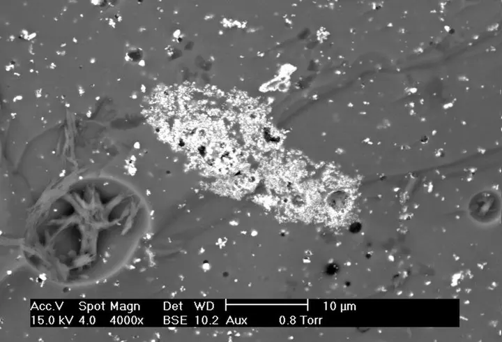

According to Goldstein and other experts, if a sample is non-conductive, it acts like an electron mirror, a phenomenon known as 'charging'. It is precisely to eliminate this problem that metal coating is essential. Sometimes, biological samples are also made conductive using osmium. Modern technology now also employs Cryo-SEM, in which the sample is frozen at extremely low temperatures. This method has proven to be a boon for the study of temperature-sensitive substances such as fats or ice.
SEM is not limited to just taking images. Features such as Energy Dispersive X-ray Spectroscopy (EDS) can be added to it. When the electron beam removes electrons from the inner part of the sample's atoms, X-rays are emitted. By measuring the wavelength of these X-rays, it can be determined which elements (such as iron, silicon, carbon) are present in the sample and in what quantities. In this way, SEM becomes a powerful analytical tool, which is widely used in forensic science, material science, and the semiconductor industry.

In countries like India, the use of SEM is continuously increasing in nanotechnology and pharmaceutical research as well. This technology is essential for measuring the particle size of new drugs or for examining the properties of new materials. To the general public, this might seem like a complex machine, but SEM plays a major role in verifying the design and quality of the microchips inside the smartphones we use. It shows us wonders of nature that we could never have seen with the naked eye.
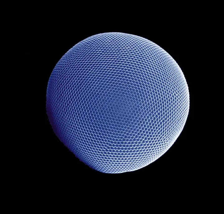
Finally, SEM technology is still evolving. Thanks to new field emission sources, it is now possible to obtain brighter and more stable electron beams that can operate for longer periods. As science advances, we will be able to observe this invisible world of nanometers with greater depth and clarity. SEM has proven that if the perspective of observation changes (electrons instead of light), the entire world changes.