A Window to the Atomic World: How the Scanning Tunneling Microscope Makes the Invisible Visible
Awarded the Nobel Prize in 1986, this technology leverages the laws of quantum physics to provide the ability to view and manipulate individual atoms.
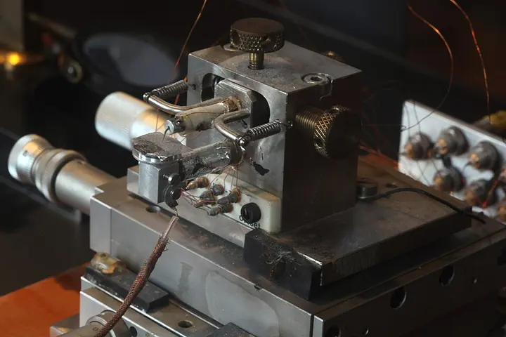
In the history of science, there are certain discoveries that fundamentally transform humankind's ability to observe. The Scanning Tunneling Microscope (STM) is one such revolutionary invention. Developed in 1981 by Gerd Binnig and Heinrich Rohrer at IBM Zurich, this instrument allowed scientists for the first time to view the surface of matter at the atomic level. For this unprecedented achievement, they were awarded the Nobel Prize in Physics in 1986. According to Wikipedia reports, the STM is not merely a powerful magnifying glass, but it possesses the capability to 'image' individual atoms on the surface of matter without touching them and to relocate them.
Conventional microscopes use light rays and lenses, but the STM operates on a completely different principle. It is based on a peculiar law of physics called quantum tunneling. According to classical physics, if a particle does not have sufficient energy, it cannot cross a barrier. However, in the world of quantum mechanics, particles like electrons can 'tunnel' through an extremely thin barrier, even if they do not possess enough energy to surmount it. In the STM, this barrier represents the empty space or vacuum between the microscope's sharp tip and the surface of the material. When this tip is brought extremely close to the surface and a voltage is applied between them, electrons pass through this empty space, which is referred to as the tunneling current.
- Coarse ApproachThe microscope tip is mechanically brought extremely close to the surface, typically observed visually.
- Bias VoltageA small bias voltage is applied between the tip and the sample surface to allow electrons to flow.
- Piezo ElongationThe piezoelectric scanner slowly elongates until a tunneling current begins to flow between the tip and the surface.
- Tunneling EstablishmentThe tip is stabilized at a distance of 4 to 7 angstroms (0.4-0.7 nm) from the surface, where attractive forces are active.
- Raster ScanningThe tip moves in an x-y matrix on the surface and creates a digital image by recording changes in current or height.
The most critical component in the construction of this microscope is its tip. This tip is generally fabricated from a tungsten or platinum-iridium wire. Ideally, the point of this tip should be so fine that there is only a single atom at its extremity. According to Wikipedia sources, an electrochemical etching method is used to produce a tungsten tip, while a platinum-iridium tip is made by mechanical cutting. The sharper the point of this tip, the higher the resolution or clarity of the microscope. The STM can resolve details smaller than 0.1 nanometer (nm) and its depth-measuring capability is as precise as 0.01 nanometer.
A piezoelectric scanner is used to move the tip across the surface with extreme precision. Piezoelectric materials are those that contract or expand when an electrical pressure, or voltage, is applied to them. In an STM, a tube made of lead zirconate titanate ceramic is generally used. By changing the voltage across this tube, the tip can be moved at the nanometer level in all three directions: x, y, and z. This technology is so sensitive that it can achieve movement of approximately 5 nanometers per volt. It is due to this precision that scientists can accurately measure the depressions and elevations on the surface or the arrangement of atoms.
| Parameter | Value / Detail |
|---|---|
| Lateral Resolution (Width) | Less than 0.1 nanometer (nm) |
| Depth Resolution (Depth) | 0.01 nanometer (10 pm) |
| Tip-sample distance | 4 to 7 Angstroms (Å) |
| Piezoelectric constant | 5 nanometers per volt |
| Tip material | Tungsten, Platinum-Iridium, Gold |
| Scanning matrix | 128x128 to 1024x1024 pixels |
The STM primarily operates in two modes: constant-current mode and constant-height mode. In the constant-current mode, the electrical current between the tip and the surface is maintained at a fixed level. As the tip moves across the surface, changes in height occur due to the surface atoms. This change causes the current to vary, which is immediately corrected by feedback electronics, and the tip is moved up or down. In this way, an image of the surface is generated by mapping the path the tip travels. On the other hand, in the constant-height mode, the height of the tip is kept constant and the variations in current are measured directly. This mode is faster, but if the surface is rough, there is a risk of the tip colliding with the surface.
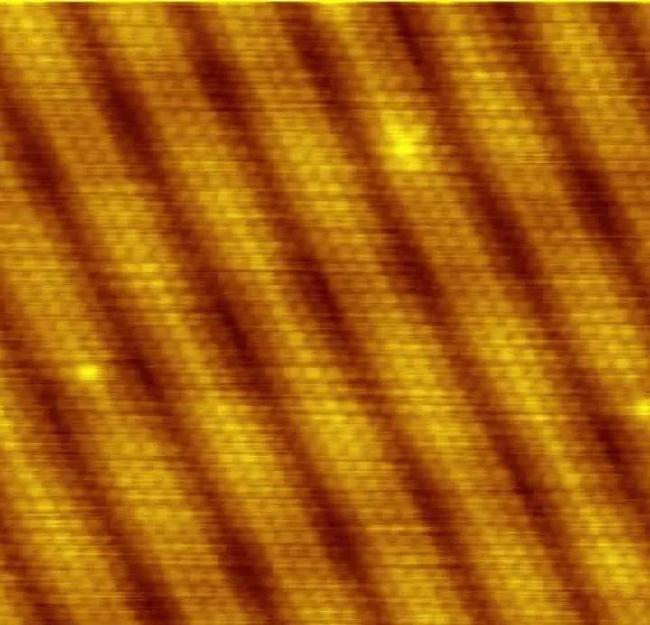
The biggest challenge for this microscope is external vibration. When working at the atomic level, the vibration of a ceiling fan in the room or the sound of a truck passing at a distance can also interfere with the experiment. Therefore, the STM is placed on an extremely complex vibration isolation system. While earlier models used magnetic levitation platforms, modern systems use mechanical springs or gas springs. Some extremely sensitive microscopes are even kept in anechoic chambers, which are completely free from sound and electromagnetic waves.
નેનોમીટર (nm)
Beyond merely capturing surface images, STM is also used for Scanning Tunneling Spectroscopy (STS). In this method, the tip is held stationary at one point while the voltage is varied and the resulting changes in current are recorded. This provides information about the energy of electrons within the material and their density of states. Such information is extremely important in nanotechnology and semiconductor research. Furthermore, by using the STM tip, individual atoms on a surface can be moved from one place to another. This process is called atomic manipulation, which paves the way for building atomic-scale machines in the future.

The operation of STM also requires a vacuum and precise temperature control. Most STMs operate in ultra-high vacuum so that air molecules do not deposit on the surface, keeping it completely pristine. Many experiments are conducted at temperatures close to absolute zero, or near zero degrees Kelvin, so that atomic motion is minimized and stable images can be obtained. However, specialized STMs capable of working in air, water, or at temperatures exceeding 1000 degrees Celsius have also been developed. The images captured by this instrument are fundamentally grayscale, but colors are subsequently added via computer to make them easier to interpret.

In countries like India, where research in nanotechnology and materials science is growing, instruments like the STM are indispensable. Although these instruments are extremely expensive and difficult to maintain, Wikipedia notes that many hobbyists are now building simple STMs at home. This tool has given us the power to understand how nature is organized at the atomic level. In the future, when we build faster computer chips or new medicines, the knowledge gained through the STM will form the foundation. This is not merely a microscope, but our passport to enter the nano-world.