Carving Stone with Light: The Science of Silicon Chips and Photolithography
How are billions of transistors etched onto silicon wafers made from sand? The complete story of ultraviolet rays, chemical reactions, and ultra-fine nanometer-scale fabrication.
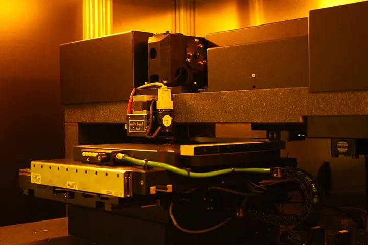
Modern human civilization today rests on the invisible foundation of silicon chips. The microprocessors pulsing inside smartphones, computers, cars, or supercomputers actually contain billions of extremely microscopic switches, namely transistors. These structures, thousands of times thinner than the thickness of a human hair, cannot be built using any mechanical tool or needle. The wondrous technology used for their manufacturing is called semiconductor device fabrication and specifically photolithography. This is a process in which rays of light are used to print highly complex electronic circuits onto a layer of silicon.
In the Greek language, "photo" means light, "litho" means stone, and "graphy" means writing or imaging. This term is derived from the traditional lithographic printing method done with ink on limestone in ancient times. However, in modern electronics, this "stone" means a thin disc of ultrapure silicon crystal, which is called a wafer. With the help of photolithography, designs of nanometer scale (nanometer: one billionth of a meter) are prepared on this wafer. This entire manufacturing process takes place in highly specialized facilities known as fabs or foundries.
Cleanroom and Manufacturing Environment
A semiconductor chip manufacturing factory is not like ordinary industrial units. Its main part is called a cleanroom. Even a simple dust particle floating in the air, if it settles on the wafer, can destroy the circuit of the entire chip. Therefore, the air in the cleanroom is continuously purified through ultra-fine filters. Scientists and engineers working there wear special suits covering them from head to toe.

Inside the fabrication plant, silicon wafers are not taken out into the open air. They are transported in specially sealed plastic boxes called FOUP (Front Opening Unified Pod). An inert atmosphere of nitrogen gas is maintained inside these boxes so that the copper wiring does not undergo oxidation. To insert these specialized boxes into the processing machine, a system named Equipment Front End Module (EFEM) is used, which provides an even purer environment to the wafer than the external cleanroom. The manufacturing of chips with state-of-the-art 7, 10, or 14 nanometer nodes takes an average of 11 to 13 weeks, and in certain complex stages, this period can reach up to 15 weeks.
Working Mechanism of Photolithography: Circuit Patterning by Light
The basic process of photolithography is very similar to photography. Just as photos were developed by exposing negative film to light in old-fashioned cameras, circuit designs are etched onto a silicon wafer here. The entire process is divided into specific, sequential stages.
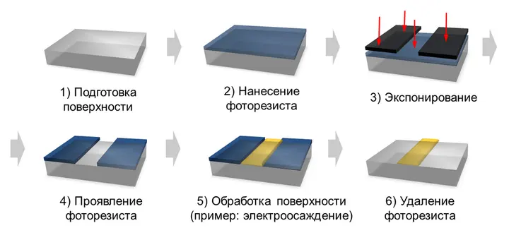
First, the wafer is chemically cleaned. To remove organic or inorganic impurities from the surface, the ‘RCA clean’ method using a solution containing hydrogen peroxide, or acetone, trichloroethylene, or methanol is used. Afterwards, the wafer is heated at 150 °C for ten minutes to remove surface moisture. Because the silicon dioxide on the wafer attracts liquids, a chemical called hexamethyldisilazane (HMDS) is applied so that the photoresist adheres strongly to it. This chemical makes the surface extremely water-repellent, much like car wax.
Next, a liquid photoresist (a chemical layer sensitive to light) is spread by spin coating. The wafer is spun at an extremely high speed so that excess chemical is thrown off due to centrifugal force, forming an extremely thin, uniform layer on the surface. For designs smaller than 125 nanometers, the photoresist layer is kept even below 0.5 microns. After spinning, the wafer is prebaked at 90 to 100 °C for 30 to 60 seconds so that the solvent evaporates.
Now comes the main stage: exposure. A photomask (a glass or quartz plate containing the original circuit design) is placed in an extremely precise machine called a stepper or scanner. Intense light is projected from the mask onto the wafer. The incidence of light causes chemical changes in the photoresist. In positive resist, the illuminated part becomes soluble in a liquid called ‘developer’ and is washed away, whereas in negative resist, the unilluminated part dissolves. Chemically amplified resists (CAR) are used in deep ultraviolet (DUV) processes, where colliding photons generate acid that accelerates the reaction.
- Cleaning and preparationThe silicon wafer is chemically cleaned and coated with HMDS.
- Spin coatingA thin layer of liquid photoresist is applied to the wafer.
- ExposureThe circuit design is printed by shining intense light through a photomask.
- DevelopmentUnprotected areas are washed away with a solvent to reveal the design.
After development, processes such as etching (corroding and removing excess material using acid or plasma), ion implantation (altering electrical conductivity by adding impurities), or deposition (depositing new metal or insulating layers) are performed on the newly exposed design. To create a single complex integrated circuit, the same wafer must go through such a photolithography cycle about 50 times.
Historical Journey: From Natural Asphalt to Superchip
The use of light-sensitive materials began in the 1820s with Nicephore Niepce. He used a natural asphalt called 'Bitumen of Judea' as the world's first photoresist. In 1940, Oskar Süß created the first positive photoresist using diazonaphthoquinone. In 1954, Louis Plambeck developed the dycril polymeric plate.
The foundation of lithography in the semiconductor sector was laid in the 1950s. In 1952, J. W. Lathrop and James R. Nall were assigned the task by the U.S. Army of miniaturizing electronic circuits for a proximity fuze. Inspired by a liquid used to mark rivet hole boundaries in aircraft wings, they developed this method to protect germanium transistors and pattern them using light. At a conference in Washington, D.C. in 1958, they used the term 'photolithography' for the first time. They preferred this term over 'photoetching' because it sounded more high-tech. Their patent for this was approved on June 9, 1959.
Around this same period, in 1955 at Bell Labs, Carl Frosch and Lincoln Derick accidentally developed a silicon dioxide layer on silicon and noted its surface passivation effects. In 1957, using a masking method, they built the world's first planar field-effect transistors (FETs), in which the drain and source were adjacent on the same surface. Also in 1957, Jules Andrews of Bell Labs obtained a patent for semiconductor photolithography. In 1963, CMOS technology was invented, which the RCA company developed commercially starting from 20 microns down to 10 microns in 1968.
Scaling Size: From 1-Inch to 300-Millimeter Wafers
As the demand for electronic devices grew, the diameter of silicon wafers was increased to manufacture more chips simultaneously. A larger wafer size allows a greater number of dies (a single chip cut and separated from the wafer) to be obtained at one time, which reduces manufacturing costs.
In the 1960s, the wafer size was only 25 mm (1 inch). At that time, engineers handled wafers using tweezers. In the 1970s, vacuum wands and wafer cassettes arrived. With the advent of 150 mm wafers, manual handling became hazardous and robotics became essential. Since the year 2000, 300 mm wafers have become the global standard. Today, older and simpler chips (such as analog or power ICs) are produced on 200 mm wafers, while state-of-the-art processors are produced exclusively on 300 mm wafers.
મિમી
Process Nodes and Modern Geopolitics
In the semiconductor industry, 'process size' or 'feature size' refers to the minimum linewidth that can be etched onto a chip. Historically, names like 90 nanometers or 350 nanometers represented the gate length of a transistor. However, after 1994, this metric became more of a marketing term. For example, Intel's 10-nanometer process actually features FinFET end widths of 7 nanometers, which has the exact same transistor density as TSMC's 7-nanometer process.
Today, manufacturing nanometer-scale chips requires light with extremely short wavelengths. The Netherlands-based company ASML holds a global monopoly on building Extreme Ultraviolet Lithography (EUVL) machines. These machines are so sensitive and strategic that in 2019, the Trump administration exerted pressure to ban the sale of EUV machines to China by ASML. Amidst this technological competition, in 2026, a domestic Chinese company began shipping Deep Ultraviolet (DUV) immersion lithography tools to customers. According to analyst Gregory C. Allen, China expects to build 5 and 20 immersion machines in 2026 and 2027 respectively, which aligns with the pace of the 13 machines put out for commercial evaluation by ASML during 2003-2005.
| Year | Expected number of machines to be built |
|---|---|
| 2026 | 5 |
| 2027 | 20 |
For countries like India, making inroads into the semiconductor fabrication sector is not merely an economic matter, but a question of geopolitical autonomy. Everything from smartphones to defense systems relies on these silicon wafers. The scientific art of extracting pure silicon from sand and printing billions of transistors upon it in microscopic dimensions using ultraviolet light waves is one of the most intricate and impressive achievements in human history.