Google's 8th Generation Tensor Chips: A Foundational Revolution for Autonomous AI Agents
Google has charted a new course for the future of artificial intelligence with its new TPU 8tx and TPU 8i Max chips, specifically engineered for complex agentic tasks.
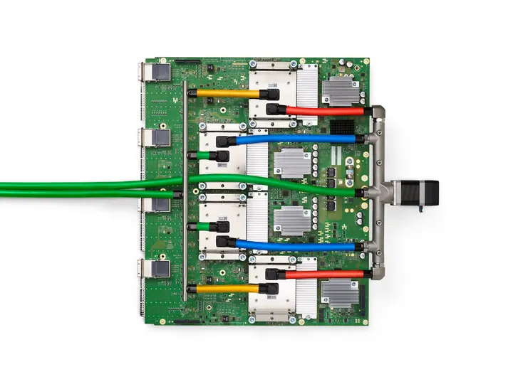
The world of Artificial Intelligence (AI) is currently undergoing a major transformation. Until now, we were using AI only to get answers to questions or to generate images, but now the era of 'AI agents' is arriving. These agents are autonomous programs that do not just provide answers, but can also perform complex tasks on behalf of the user. To meet these changing needs, Google has announced its eighth-generation Tensor Processing Unit (TPU). According to company reports, these new chips have been designed specifically with agentic workloads in mind—that is, tasks where AI must make decisions and take actions on its own.
Google's new announcement includes two main chips: the TPU 8tx and the TPU 8i Max. According to a Business Standard report, Google expanded this series on November 10, 2026, which is designed to support secure AI inference—the process of drawing conclusions from data—and complex agent tasks. This is the first time Google has split its TPU architecture into separate, specialized designs for training and inference. This strategic shift indicates that AI models have now become so vast and complex that a single type of chip is no longer sufficient for all tasks.
It is necessary to understand what a TPU is. According to Wikipedia, a Tensor Processing Unit is an Application-Specific Integrated Circuit (ASIC) developed by Google specifically for neural network machine learning. Compared to a standard Graphics Processing Unit (GPU), a TPU is designed to perform low-precision calculations very quickly and with lower power consumption. Google began using these chips internally in 2015 and has made them available to other companies via cloud services since 2018. These chips are developed in collaboration with the company Broadcom and are manufactured by the Taiwan Semiconductor Manufacturing Company (TSMC).
Two separate paths: Training and Inference
Google announced its eighth-generation TPU on April 22, 2026. This generation consists of two main types: TPU 8t and TPU 8i. Here, 't' stands for training, the process of teaching a model, while 'i' stands for inference, the process of obtaining results using a trained model. Both chips are hosted on Google's proprietary Arm-based Axion CPUs and utilize fourth-generation liquid cooling technology.
The TPU 8t is designed for the pre-training of large-scale frontier models. Its capacity is remarkable. It delivers a peak performance of 12.6 FP4 PFLOPs (petaflops). FP4 is a 4-bit floating-point format that increases computation speed. It features 216 GB of HBM3e memory, which provides a bandwidth—the speed of data transfer—of 6,528 GB/s. These chips are connected via the 'Virgo Network,' allowing for the creation of a 'SuperPod' of 9,600 chips. This SuperPod possesses a massive total computational power of 121 FP4 ExaFLOPs.
On the other hand, the TPU 8i is prepared for high-speed serving and AI agents. Since AI agents require long-duration reasoning, this chip is equipped with 288 GB of HBM3e memory, with a bandwidth of 8,601 GB/s. Most importantly, it features 384 MB of on-chip SRAM (Static Random Access Memory), which is three times larger than the previous generation. This memory keeps data very close to the processor, thereby increasing processing speed. It utilizes the 'Boardfly' network topology and a Collectives Acceleration Engine (CAE), which reduces synchronization latency—the delay between two tasks—by a factor of five.
| Detail | TPU 8t (Training) | TPU 8i (Inference) |
|---|---|---|
| Peak Performance | 12.6 FP4 PFLOPs | 10.1 FP4 PFLOPs |
| HBM Memory Capacity | 216 GB | 288 GB |
| Memory Bandwidth | 6,528 GB/s | 8,601 GB/s |
| Network Fabric | Virgo Network | Boardfly Topology |
The Science Behind the Technology: Systolic Arrays
To understand how a TPU works, one must visualize a 'systolic array.' Just as the heart pumps blood in the human body, data in this architecture flows continuously through a network of processors. In a standard processor, data must be sent back to memory after every calculation, but in a TPU, the result of one calculation goes directly to the next processor. This reduces the need for memory access and lowers power consumption. An engineer named Norman Jouppi led this design, proving that TPUs can provide 30 to 80 times more efficiency than other processors.
- Data InputData is sent to the TPU via the PCIe bus by the host processor (CPU).
- Systolic Array ProcessingData passes through matrix multiplier units, where the result of one processor goes directly to the next.
- Activation FunctionAn activation function is applied to the calculated data so the neural network can make a decision.
- Result OutputThe final result or conclusion is sent back to the memory or the host processor.
Looking at the history of Google, this company was founded in 1998 by Larry Page and Sergey Brin. In 2015, Sundar Pichai became the CEO of Google, and under his leadership, Google pivoted to becoming an 'AI-first' company. The development of the TPU is a key part of this strategy. The first-generation TPU was announced at the 2016 Google I/O conference. Since then, every generation has seen a major leap in performance. For example, the fourth-generation TPU v4 was claimed to be 5% to 87% faster than the Nvidia A100. Now, with the eighth generation, Google is directly competing with Nvidia's state-of-the-art H100 and subsequent chips.
Importance for the general public and India
You might wonder what benefit these chips have for the common man. When you perform a Google search, look for photos in Google Photos, or use Google Translate, it is these TPU chips working behind the scenes. A single TPU in Google Photos can process over 100 million photos in a day. With the arrival of the new 8th-generation chips, AI agents will become more accurate and faster. In the future, the AI agent on your phone will be able to perform tasks ranging from booking your flight to handling your entire office workload in an instant, as it will be supported by such powerful chips in the cloud.
For a country like India, where the reach of digital services is growing, the use of these TPU chips via Google Cloud could prove to be a boon for Indian startups and researchers. The massive computational power required to train Large Language Models (LLMs) for Indian languages can be provided by these TPU 8s. Furthermore, Google is now in talks with companies like Meta to use TPUs in their data centers, which means that in the future, AI features on Facebook or Instagram could also run on these Google chips.
GB/s
In conclusion, Google's 8th-generation TPU is not just a hardware upgrade, but a preparation for a new era of AI. By creating separate chips for training and inference, Google has proven that it intends to maintain its dominance in the AI field. As AI agents become an integral part of our lives, the role of these chips will become increasingly decisive. While it remains to be seen how secure this technology will be and what its cost will be, for now, Google has set a new benchmark in the world of semiconductors.