India's Semiconductor Revolution from Dholera and Sanand: The Science of Chip Fabrication and Gujarat's Role
The extremely complex technology of carving billions of transistors onto a silicon wafer is now taking shape on the soil of Gujarat. The Dholera Special Investment Region and the future of the semiconductor industry.
The Rise of the Silicon Revolution in Gujarat
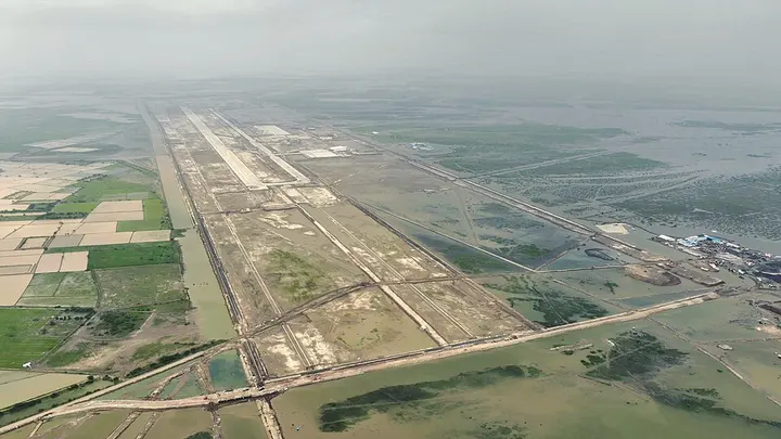
Today, the invisible silicon chip has become the driving force of modern human civilization and economy. Smartphones, cars, supercomputers, or defense equipment—every sector comes to a standstill without semiconductors. On this global stage, India has taken its largest leap in domestic chip manufacturing from Dholera and Sanand in Gujarat. Located approximately 100 kilometers south-west of Ahmedabad district in the Dholera Special Investment Region (DSIR), India's first chip fabrication plant is being established by the Tata Group. Alongside this, the Vedanta Group is also engaged in discussions for an initial phase investment of $5 billion with three partners for a display and semiconductor fab.
This project is not limited merely to building factories, but marks India's official entry into the world's most complex industrial manufacturing sector. To enter this sector, which has hitherto been dominated by countries like the US, Taiwan, and South Korea, a new greenfield industrial city spanning over 920 square kilometers is being built in Dholera, Gujarat. To understand why semiconductor manufacturing is so difficult and what is being built in Dholera, it is essential to delve into the core of its science and manufacturing process.
The Science of Chip Fabrication: From Wafer to Die
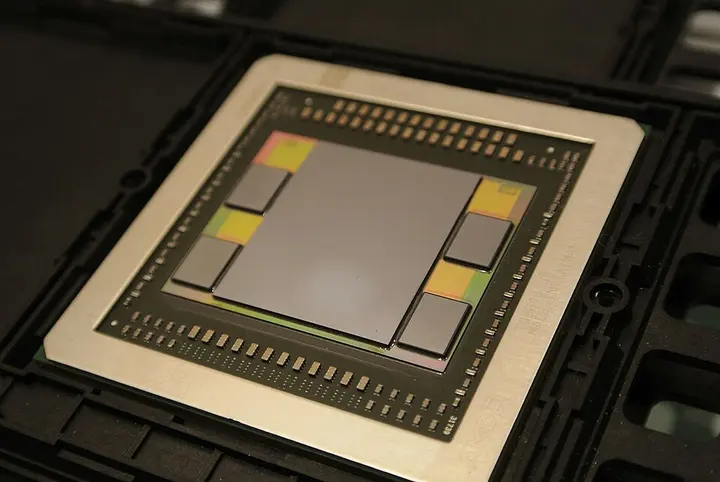
Semiconductor device fabrication is fundamentally a multi-step process of creating Integrated Circuits (ICs). In this process, a circular disc made of pure single-crystal semiconductor material, called a wafer, has thousands to crores of electronic circuits prepared on it sequentially. This manufacturing takes place in highly specialized plants called foundries or 'fabs'. The heart of a fab is its 'clean room', where the concentration of dust particles in the air is kept near zero, because even a single tiny dust particle can destroy a microscopic circuit.
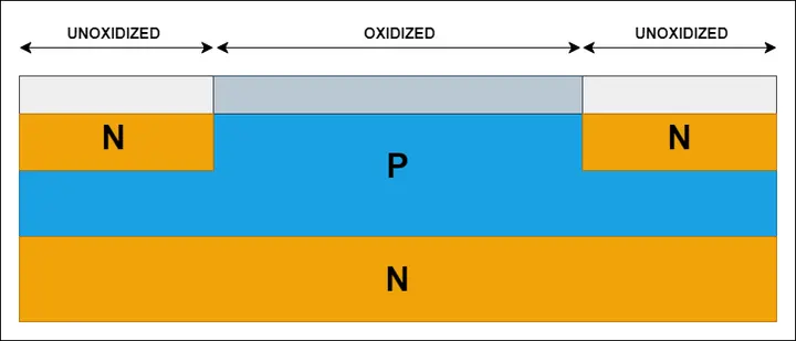
This process is a complex cycle of photolithography (a technique of printing designs on a chemical surface using light) and physical-chemical processes. It involves steps like thermal oxidation (forming an oxide layer on silicon), thin-film deposition, ion implantation (adding ions to control current flow in silicon), and etching (chemically carving away unnecessary parts) repeated over and over. Countless integrated circuits are built on a single finished wafer, which are called dies. After the process is complete, the wafer is cut to separate these dies, which is called die singulation or wafer dicing, and then it is packaged.
- 1. Wafer selectionThe creation of circuits begins on a circular disc (wafer) made of pure single-crystal semiconductor material.
- 2. Clean room processingPhotolithography and physical-chemical processes are carried out in a clean room with zero dust particles.
- 3. Circuit manufacturingThousands to crores of circuits are formed on the wafer through thermal oxidation, deposition, ion implantation, and etching.
- 4. Die singulation and packagingThe completed wafer is cut to separate the dies and finally packaged.
- Thermal oxidation and thin-film depositionA protective oxide layer is formed on the surface of pure single-crystal silicon wafer and ultra-thin layers of necessary chemical substances are applied.
- PhotolithographyThe ultra-fine design of the chip's circuit is precisely printed (patterned) onto the wafer surface with the help of light and a mask.
- Etching and ion implantationUnnecessary parts are carved out and removed by chemical processes (etching) and impurity ions are introduced into silicon to alter its electrical properties.
- Metal wiring and mini-environment handlingTransistors are interconnected through conductive metals like copper; the wafer is transported from one machine to another in a FOUP box containing a nitrogen atmosphere.
- Die singulation and packagingAfter an 11 to 15 week process, the wafer is cut to separate individual chips (dies) and sent for final assembly and packaging.
Highly Controlled Environment and Machinery
In modern fabrication, wafers are never exposed to ordinary air. Inside the plant, wafers are transported in specialized sealed plastic boxes called FOUPs (Front Opening Unified Pods). A pure nitrogen atmosphere is maintained inside these FOUP boxes so that the copper used for wiring on the wafer does not oxidize. The atmosphere inside the processing equipment and the FOUP is even purer than the clean room air, which is known as a 'mini-environment'.
This mini-environment is connected to an EFEM (Equipment Front End Module), which allows the machine to accept the FOUP and introduce the wafer inside. An air curtain or barrier is arranged between the FOUP and EFEM to prevent moisture from the air from entering. To keep all this equipment and FOUPs continuously purged with nitrogen, fabrication plants require massive quantities of liquid nitrogen. In the world, only a handful of giant companies like ASML, Applied Materials, Tokyo Electron, and Lam Research are capable of building such fabrication machinery.
The fabrication of chips running on modern 14, 10, or 7 nanometer (nm) nodes takes an average of 11 to 13 weeks, while advanced processes can take as long as 15 weeks. This production is fully automated, with material handling systems transporting wafers from one machine to another.
અઠવાડિયા
The Historical Journey of Wafer Sizes and Nodes
The history of semiconductor technology has been one of continuous shrinking and expanding—transistors got smaller and wafers got bigger. It began in 1960 with a wafer of just 25 millimeters (1 inch). In 1969 it became 50 millimeters (2 inches), in 1976 100 millimeters (4 inches), in 1981 125 millimeters (5 inches), and in 1983 150 millimeters (6 inches). In 1990 came the 200-millimeter (8-inch) wafer, which became widespread in 1992, and by the year 2000, the 300-millimeter (12-inch) wafer became the global standard.
મિલીમીટર (mm)
In the era of early 2-inch wafers, workers held wafers manually using tweezers. Then came vacuum wands and wafer cassettes. Reaching 150 millimeters made robotics indispensable, as 200-millimeter cassettes became heavy, making manual handling hazardous. Today, the 300-millimeter wafer reduces production costs by providing more surface area, although 200-millimeter wafers are still used today for analog ICs, RF chips, and power devices.
The foundation of this revolution was laid in 1955 at Bell Telephone Laboratories, when a layer of silicon dioxide was accidentally formed on a silicon wafer by Carl Frosch and Lincoln Derick. By 1957, they built the first planar field-effect transistor. Subsequently, in 1959, Jean Hoerni developed the planar process at Fairchild. In 1963, Chih-Tang Sah and Frank Wanlass developed CMOS technology, which was scaled by RCA in 1968 in 4000-series circuits starting from 20 micrometers down to 10 micrometers.
Over time, nomenclature based on the gate length of the transistor began as a 'technology node' (such as the 90 nm process). However, after 1994 and especially after 2009, the nanometer (nm) ceased to be a physical measurement and became merely a marketing term. For example, Intel's 10 nm process has a FinFET fin width that is actually 7 nm, possessing the exact same transistor density (number of transistors per unit square area) as TSMC's 7 nm process.
The Global Industry and the Selection of Dholera SIR
Currently, the semiconductor industry is a fully global business. The world's largest pure-play foundry, TSMC, has facilities in Taiwan, China, Singapore, and the USA. Samsung has plants in South Korea and the USA, while Intel is spread across Europe, Asia, and the USA. On the other hand, fabless (without their own factories) companies like Qualcomm and Broadcom only design chips and have them manufactured by foundries like TSMC.
Establishing such a highly sensitive industry requires uninterrupted electricity, ultra-pure water, earthquake-free land, and global logistics connectivity. The Dholera Special Investment Region (DSIR) of Gujarat has been shaped for this very purpose. Announced in 2013 by the then Chief Minister of Gujarat, Narendra Modi, this project is being developed as a joint initiative of the Government of India and Japan within the influence zone of the Delhi-Mumbai Industrial Corridor (DMIC).
Under the Special Investment Region Act 2009 enacted by the Government of Gujarat, the 'Dholera Special Investment Region Development Authority' (DSIRDA) was established in 2019. For the implementation of this project, a Special Purpose Vehicle (SPV) named 'Dholera Industrial City Development Limited' (DICDL) was formed on January 28, 2016, by the Government of India (DMIC Trust) and the Government of Gujarat (DSIRDA), in which the Government of Gujarat holds a 51% stake and the Government of India holds 49%.
| Project / Component | Main Detail / Capacity | Partnership / Agency |
|---|---|---|
| Total planned area | More than 920 square kilometers | Central and Gujarat Governments |
| Managing SPV (DICDL) | 51% Gujarat Government (DSIRDA), 49% Central Government (DMIC) | DICDL |
| Ultra-Mega Solar Park | 4400 MW (Phase-1: 1000 MW, 300 MW commissioned) | Tata Power / Government |
| Ahmedabad-Dholera Expressway | 109.019 km greenfield road | National Highways Authority |
| International Airport | Greenfield airport (Target: 2026) | DICDL / Airport Authority |
| Semiconductor Chip Fab | India's first chip fabrication unit | Tata Group |
| Semiconductor / Display Fab | Proposed investment of $5 billion in the first phase | Vedanta Group |
Plug-and-Play Infrastructure and Green Energy
A 'plug-and-play' (ready infrastructure facilities) model has been prepared to attract chip manufacturers to Dholera. Fab plants require billions of kilowatts of electricity. To meet this demand, an ultra-mega solar park of 4400 megawatts (MW) capacity is being built in Dholera, of which the first phase of 1000 MW is under implementation and 300 MW capacity has been commissioned by Tata Power.
The 109.019-kilometer-long Ahmedabad-Dholera Greenfield Expressway is being opened for public use in 2026 for the fast and secure transportation of chips. In addition, a freight rail network between Bhimnath and Dholera and a new greenfield international airport are under construction, targeted to be operational by 2026. Global interest is also increasing; in 2023, South Korean companies explored investment possibilities here, while a 12,095 square meter plot was allocated for the first five-star hotel in the hospitality sector. In the Gujarat Data Center Policy 2026-29 announced in July 2026, Dholera has been declared a primary hub with a capacity of 7 to 8 gigawatts and an investment potential of ₹6 to 7 lakh crore.
Social Challenges and Land Acquisition Dispute
Construction of massive industrial cities is not possible without questions from local communities. Between 2009 and 2022, farmers of about 22 villages in the Bhal region of Dholera staged widespread protests against land pooling. Forming organizations like the 'Bhal Bachao Samiti', farmers demanded the enforcement of farmer consent provisions under the Land Acquisition Act of 2013.
The primary protest of the farmers was that under the SIR Act, 50% of their land was taken and in return smaller or flood-prone land was allocated. Furthermore, incidents like rallies, sit-ins, hunger strikes, and detentions took place against the loss of fertile agricultural land and compensation given on the basis of old jantri. However, despite these protests, the government proceeded with surveys and issued notices to advance the land acquisition process of the project.
The Path Ahead for India
Semiconductor plants beginning in Sanand and Dholera will not only strengthen the local electronics supply chain but also establish India on the global chip manufacturing map. Processes used in fabrication are also useful in the manufacturing of other devices such as displays (LCD and OLED). The journey that began with planar transistors has now reached the creation of billions of circuits on 300-millimeter wafers in the clean rooms of Gujarat. This journey depends on the harmony of extremely complex equipment, precise chemical processing, and massive infrastructure.