A New Revolution in Chip Manufacturing: Why TSMC's CoWoS Technology Has Become Indispensable for AI
Amid the limitations of transistor scaling, the future of artificial intelligence now depends on advanced semiconductor packaging and Taiwan's leading companies.
Packaging is no longer just a protective shell: The cornerstone of the AI revolution
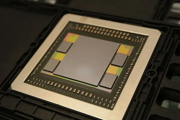
As the global race to build the infrastructure required for Artificial Intelligence (AI) intensifies, billions of dollars in semiconductor industry investment have shifted toward a field that was previously not considered very attractive in the tech world. This field is advanced packaging. In the past, the primary role of packaging was limited to protecting the silicon chip from external factors and providing electrical connections to link it to a circuit board. Today, it has become the biggest bottleneck in the manufacturing of the world's most powerful processors.
Pat Gelsinger, former Intel Chief Executive and current partner at Playground Global, recently stated in Taipei that packaging had always been something no one worried about. But now, the situation has changed completely. According to Gelsinger's estimates, today's modern graphics and central processing units incorporate 10 or more, and sometimes up to 20, separate chips connected together. Because of this, advanced packaging alone can account for half (50 percent) of the total value of an entire chip product.
In this global race, Taiwan's leading company, TSMC (Taiwan Semiconductor Manufacturing Company), holds the top position in the market with its cutting-edge Chip-on-Wafer-on-Substrate, or CoWoS, packaging technology. According to a report by market research firm Yole Group, revenue from advanced packaging is expected to surpass that of traditional packaging for the first time in 2026, and capital investment in this sector is likely to reach $28 billion. Currently, TSMC's packaging capacity is falling short of meeting the extraordinary demand for AI processors, which has created new opportunities for other semiconductor manufacturers.
The journey from traditional packaging to advanced packaging
For decades in the history of semiconductor chips, Moore's Law prevailed, which involved an effort to double the number of transistors on a silicon die (the original square piece of the processor) every two years. Transistors are the microscopic switches that control the flow of electricity. However, making these transistors smaller has now become technologically extremely complex and expensive. Fitting everything onto a single large monolithic chip increases production defects (yield degradation) and causes costs to skyrocket.
As a solution to this problem, advanced packaging has emerged, acting as a bridge between the fabrication facility (fab) and traditional packaging. Advanced packaging allows for the integration of various components into a single device. It enables heterogeneous integration, where advanced process nodes are used only for core logic processors, while older and cheaper technology is utilized for components such as analog or input-output (I/O). This methodology includes techniques such as multi-chip modules, 2.5D and 3D ICs, system-in-package, and die stacking.
- Fabrication of silicon interposerAn intermediate layer of silicon is prepared with high-density wiring and Through-Silicon Vias (TSV) for fast connections between chips.
- Connection of processor and memoryThe main processor die (GPU/CPU) and High-Bandwidth Memory (HBM) modules are placed extremely close to each other on the interposer using micro-bumps.
- Wafer-level processingThe entire assembly of interposer and chips is tested at the wafer level and integrated as a single unit.
- Installation on package substrateThe entire finished chip-on-wafer unit is mounted on the final package substrate to make it ready for connection to the motherboard.
Advanced packaging significantly increases efficiency by reducing the distance signals must travel from one chip to another. Global standards like Universal Chiplet Interconnect Express (UCIe) have also been developed to provide high-speed connections between chiplets (small specialized chips). Intel uses its silicon bridge-based EMIB technology, while TSMC relies on its silicon interposer-based CoWoS architecture.
How does CoWoS technology work?
TSMC's CoWoS (Chip-on-Wafer-on-Substrate) is a 2.5D packaging solution. In simple terms, it is a multi-story bridge on which a processing chip and ultra-fast memory modules are placed right next to each other. On a standard motherboard, the wires between the chip and memory are long, which causes latency in data transmission and wastes energy. CoWoS makes this distance negligible.
અબજ ડૉલર
In this architecture, the main processor (such as an Nvidia or AMD GPU) and high-bandwidth memory (HBM) are arranged on a silicon interposer (a silicon intermediate layer that provides high-density connections between chips). These components connect to the interposer via micro-bumps, and the interposer itself connects to the main substrate below through through-silicon vias (TSV: vertical conductive holes passing through silicon). This arrangement allows a massive amount of data to flow between the processor and memory in a fraction of a second, which is a lifeline for the training and computation of AI models.
Market data and production capacity constraints
Worldwide, Nvidia, AMD, Broadcom, as well as cloud companies developing their own AI processors, are entirely dependent on TSMC's CoWoS capacity. However, the global demand is so immense that TSMC cannot fulfill orders on its own. This shortage has opened new doors for other companies and suppliers.
According to industry sources, Nvidia is providing billions of dollars in funding to Siliconware Precision Industries (SPIL), a subsidiary of Taiwan's ASE Technology, to expand CoWoS capacity. This financial support is being used to establish new factories and packaging equipment. On the other hand, AMD has also announced an investment of over $10 billion in Taiwan's semiconductor industry as a whole, which includes partnerships with ASE, SPIL, and Powertech.
| Technology name | Developing organization | Platform type | Key feature and application |
|---|---|---|---|
| CoWoS (Chip-on-Wafer-on-Substrate) | TSMC | 2.5D silicon wafer | Connection of processor and HBM using silicon interposer; widely used by Nvidia and AMD. |
| EMIB | Intel | Silicon bridge | Reduces cost by using silicon bridges within the substrate for connections between chips. |
| Panel-Level Packaging (PLP) | Powertech (PTI) | Rectangular panel | Large panels reduce material waste; developed in partnership with Broadcom and AMD. |
| CoPoS (Chip-on-Panel-on-Substrate) | TSMC | Rectangular panel | TSMC's experimental pilot line technology for future large-scale AI packaging. |
AMD Chief Executive Lisa Su told Reuters in Taipei that CoWoS and advanced packaging are critical for high-performance computing, and the industry as a whole is in urgent need of much greater packaging capacity.
Panel-level packaging: New alternatives beyond TSMC
Due to shortages at TSMC, a significant opportunity has emerged for smaller Taiwanese supplier companies like Powertech Technology (PTI). The company's chairman, D.K. Tsai, stated that everyone is looking for an alternative to TSMC and no one wants to be completely dependent on them. Powertech is now focusing on panel-level packaging.
Traditionally, silicon wafers are round, which leads to wasted space at the edges. Panel-level packaging uses large rectangular panels instead of round wafers. This method allows for many more chips to be packaged in a single production round and significantly reduces material waste. Microsoft Azure's hardware chief, Rani Borkar, has also confirmed that panel packaging is helpful in reducing material waste for large AI chips.
Powertech is working with AMD and Broadcom to develop this technology and plans to invest $400 million in an advanced packaging joint venture with Broadcom in Singapore, where production could begin by 2028. To compete, TSMC is also developing its own panel technology, CoPoS (chip-on-panel-on-substrate), and has already prepared a pilot line, although CoWoS remains its primary weapon for now.
According to Tokyo Electron Taiwan President CG Nakama and American equipment manufacturer Applied Materials Vice President Mr. Kesapragada, advanced packaging is emerging as a massive market for semiconductor equipment companies over the next 3 to 5 years as well.
TSMC's history and global semiconductor dominance
TSMC, which leads in advanced packaging today, was founded in 1987 at the Hsinchu Science Park in Taiwan. Founded by Morris Chang, the company was the world's first dedicated contract chipmaker (foundry). The Taiwan government provided 48.3 percent of the initial capital, while the Dutch company Philips invested $58 million to take a 27.6 percent stake and provided technology transfer.
Today, TSMC holds approximately a 70 percent share of the global foundry market and, as of 2026, held the top position in market capitalization among non-American companies. In 2022, Taiwan's integrated circuit exports were worth $184 billion, which accounts for nearly 25 percent of Taiwan's GDP. The company possesses the capability to manufacture processors ranging from 2 microns to 3 nanometers, and expects to reach 2 nanometers by 2025.
To avoid potential disruptions in the global supply chain and geopolitical risks, TSMC has begun establishing new factories, including the $8.6 billion JASM fab in Kumamoto, Japan, and an investment of $12 billion in Arizona, USA. However, because advanced CoWoS packaging capacity remains largely concentrated in Taiwan, it is becoming the most sensitive hub of the global AI economy.