The Engine of Artificial Intelligence: The Architecture of H100 and Next-Generation Chips
How 80 billion transistors, transformer engines, and ultra-fast memory are powering today's advanced AI models.
The New Backbone of Artificial Intelligence
In today's modern computing world, the hardware required to run artificial intelligence and large language models has graphics processing units, or GPUs, at its very center. A GPU is a silicon chip built to solve thousands of small computations simultaneously in parallel. In this competition, NVIDIA's Hopper architecture and its H100 processor have become the center of global discussion. Announced during the GTC conference in March 2022, this processor is named after the renowned computer scientist and United States Navy Rear Admiral Grace Hopper.
This architecture represents a major technological leap compared to the earlier Turing and Ampere microarchitectures. The H100 has been specially designed to provide highly complex AI training and inference in datacenters and cloud networks. When the wave of artificial intelligence swept across the world, every major technology company rushed to purchase these chips.

Silicon Architecture and Streaming Multiprocessors
The Hopper H100 GPU is manufactured using semiconductor maker TSMC's advanced N4 process. Approximately 80 billion transistors are packed onto a tiny silicon die. The entire chip contains around 144 Streaming Multiprocessors (SM). In the language of computing, streaming multiprocessors are like small computational factories where actual calculations take place. Each SM can execute up to 64 warps (parallel groups of 32 threads) simultaneously.
To enhance computational capability, the single-precision floating-point (FP32) capacity in the H100 has been doubled, completing twice as many FP32 operations per cycle than its predecessor. Alongside this, full support is provided for the TensorFloat-32 (TF-32) format. Furthermore, special DPX instructions have been added to the SM for algorithms like Smith-Waterman and Needleman-Wunsch to accelerate biological computations and sequence alignment, delivering extraordinary speed in protein and genomics research.
- High Precision Data InputComplex mathematical calculations are entered from the layers of the neural network in the form of 16-bit floating point (FP16).
- Dynamic Precision ControlThe Transformer Engine automatically converts data into the faster 8-bit (FP8) format by checking for loss of precision in the result.
- Asynchronous Memory Transfer (TMA)Tensor Memory Accelerator delivers 5D data between main memory and shared memory without blocking the processor core.
- Parallel computation and resultStreaming Multiprocessor clusters complete matrix calculations at extremely high speed and store the result in global memory.
Transformer Engine: A New Methodology of Computation
The most significant feature of the H100 is its new 'Transformer Engine'. Most of today's AI models are based on transformer networks, which involve millions and billions of mathematical matrix multiplications. Previously, these calculations were primarily performed in 16-bit floating-point (FP16), which was highly accurate but slow. The Transformer Engine, implemented for the first time in the Hopper architecture, analyzes this in real-time during computation.
If the accuracy of the model is not adversely affected, this engine automatically reduces the computation from FP16 to the faster 8-bit floating-point (FP8) format. During this process, the engine dynamically adjusts the bits allocated to the mantissa or exponent to maintain precision. This method multiplies the training and inference speed of the model.
TB/s
Ultra-Fast Memory and TMA Architecture
No matter how fast a processor is, if it does not get data quickly from the memory, it becomes useless. The Hopper H100 uses HBM3 and HBM2e memories, offering a capacity of up to 80 GB. The HBM3 memory system provides an incredible bandwidth of 3 terabytes per second (3 TB/s), which is 50 percent faster compared to the 2 TB/s of the previous Ampere A100.
To support this speed, the Tensor Memory Accelerator (TMA) has been introduced in Hopper. TMA can directly transfer data between the global memory and shared memory without stopping the processor cores, where data dimensions of up to 5D tensors can be sent directly. This process reduces the burden on registers and SM instructions. In addition, the capacity of the combined L1 cache, texture cache, and shared memory in the chip has been increased to 256 KB, while automatic inline compression has also been added to the L2 cache.
| Parameter | Specification Detail |
|---|---|
| Manufacturing Process | TSMC N4 Process |
| Transistor Count | 80 Billion |
| Streaming Multiprocessors (SM) | Up to 144 |
| Memory Support and Maximum Capacity | HBM3 and HBM2e, up to 80 GB |
| Memory Bandwidth | 3 TB/s (HBM3) |
| L1 Cache / Shared Memory | 256 KB |
| Thermal Design Power (TDP) | 700 Watts (SXM5 Model) |
Clustering and the Need for High-Power Design
To build large supercomputers, many thread blocks have to be made to work together. Hopper features thread block clusters, in which a portable cluster of 8 blocks can be formed normally, and up to 16 blocks through special instructions. Advanced NVLink interconnects are used for fast data exchange among all these processors.
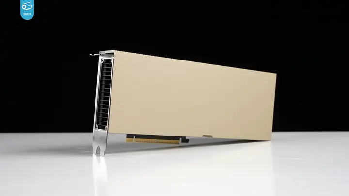
In terms of efficiency, the H100 model with the SXM5 socket has a Thermal Design Power (TDP) of 700 watts, which provides higher data bandwidth and speed than a standard PCIe socket. NVIDIA has also prepared the Grace Hopper (GH200) module using this same chip, in which a 72-core Grace CPU is connected on the same board along with the H100 GPU, and this entire module can consume up to 1000 watts of power.
Unprecedented Market Demand and Global Impacts
During the surge of artificial intelligence through 2023 and 2024, an unprecedented shortage of the H100 emerged. Larry Ellison of Oracle Corporation revealed that during a dinner with NVIDIA CEO Jensen Huang, he and Tesla and xAI's Elon Musk were practically begging for more H100 chips. According to analysts at Raymond James Financial, in January 2024 NVIDIA was selling each H100 chip at a price of $25,000 to $30,000, while on eBay these chips were selling for upwards of $40,000. By February 2024, these valuable chips were being transported to data centers in armored cars.
Meanwhile, global geopolitical discussions also commenced due to United States export controls. Modified models such as the H800 and later the H20, compliant with regulations for the Chinese market, were introduced. In early 2026, global trade disputes arose regarding the Hopper-based H200 chip, with these controls becoming a subject of discussion even during U.S. President Donald Trump's visit to China. At that time, Chinese companies such as Alibaba, Tencent, ByteDance, and JD.com were granted specific approvals to purchase the H200.
The Next Generation: The Journey from P100 to B200
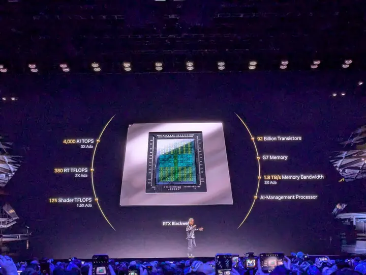
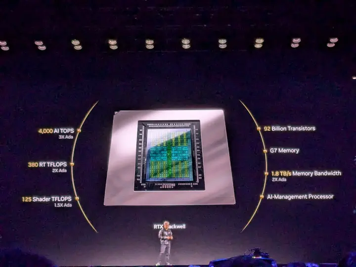
In computing history, NVIDIA's accelerator journey started with the P100 and progressed through the V100, A100, and subsequently to the Hopper H100. The next major step in this series is the Blackwell architecture along with its B200 and future R100 chips. The Blackwell series points the way toward taking AI workloads to new heights with an even larger footprint and multiple chiplets than Hopper.
Even in countries like India, where AI-based language models, healthcare, and deep learning research are rapidly expanding, the availability of such data center-grade processors is becoming a foundational necessity. As models grow larger, silicon speed and energy efficiency will dictate the science and economy of the coming decade.