Hardware Accelerators Accelerating Artificial Intelligence: Internal Architecture and Functionality of TPUs and NPUs
An in-depth analysis of specialized chips that surpass the limitations of CPUs and GPUs to accelerate AI models through systolic arrays and low-precision computing.
A New Turn in AI Computing: Why Are TPUs and NPUs Necessary?
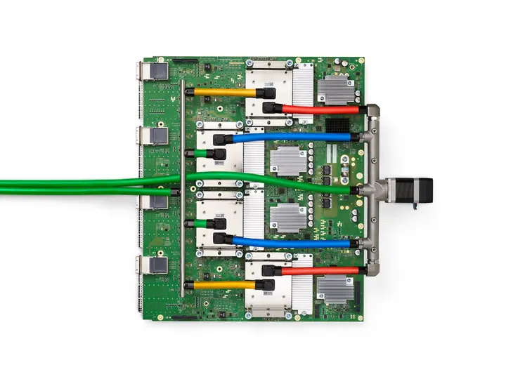
In the era of modern artificial intelligence (AI), the computational burden on traditional central processing units (CPUs) and graphics processing units (GPUs) has increased excessively. A need for special types of hardware accelerators arose to efficiently run machine learning and deep learning models. From this need, specialized application-specific integrated circuits (ASICs) such as the neural processing unit (NPU) and tensor processing unit (TPU) were born. Google began using TPUs internally in its data centers in 2015 and made them available to other companies via cloud infrastructure in 2018.
Under the leadership of Amir Salek, the founder of custom silicon development at Google, the original TPU, TPUv2, TPUv3, TPUv4, and Edge-TPU were developed. Similarly, under the technical leadership of Norman P. Jouppi, Google completed the design and deployment of the first TPU in a short span of just 15 months. According to a research paper presented at the 2017 ISCA conference, the first-generation TPU achieved 15 to 30 times higher performance and 30 to 80 times higher performance-per-watt (efficiency per watt) compared to contemporary CPUs and GPUs.
ગણું વધુ
TPUs are specifically optimized for software frameworks such as TensorFlow, JAX, and PyTorch. Google has successfully used them in complex projects such as AlphaGo, AlphaZero, Google Street View text processing, Google Photos (where one chip can process over 100 million photos per day), and RankBrain.
Systolic Arrays and Computational Architecture: How Do These Chips Work?
The main difference between TPUs/NPUs and traditional processors is their internal computational design. These chips are designed for high-volume and low-precision computation, such as 8-bit calculations. They do not have specialized hardware for rasterization or texture mapping, but they focus on delivering more input/output operations per joule.
The heart of the TPU architecture is the 'systolic array.' According to Jonathan Ross, a founding engineer at Google and founder of Groq, three different groups were working on AI accelerators at Google, of which the systolic array design proved to be the best. In this architecture, data flows continuously through a grid of processing elements like a heartbeat, eliminating the need to repeatedly read from or write to memory.
- Data inputData enters the grid of processing elements simultaneously.
- Pipeline processingData flows continuously from one element to another like a heartbeat.
- Memory savingData is processed inside the chip rather than frequently writing to or reading from memory.
- 1. Input transferHost processor sends data and machine learning instructions to TPU via PCIe bus.
- 2. Systolic array processingData passes through a 256×256 multiplier grid where parallel calculation occurs.
- 3. Accumulation32-bit accumulators collect intermediate results of calculations.
- 4. Activation and outputFinal processed data is sent back to the host system after applying activation functions.
Different processors are used in different ways for machine learning models. TPUs are highly suited for Convolutional Neural Networks (CNNs), while GPUs are more appropriate for fully connected networks and CPUs for Recurrent Neural Networks (RNNs). In Large Language Models (LLMs), it has been standard practice to use TPUs for inference and GPUs for training transformer networks.
The development journey and technical specifications of eight generations of Google TPUs
The first generation of Google TPU was an 8-bit matrix multiplication engine based on a 28 nm process, with a die size of 331 mm² or less. It operated at a clock speed of 700 MHz and 28 to 40 watts of power. It featured 28 MiB of on-chip memory and 4 MiB of 32-bit accumulators for a 256×256 systolic array, along with 8 GiB of DDR3 memory with 34 GB/s bandwidth.
The second generation (TPU v2), announced in May 2017, utilized 16 GB of High Bandwidth Memory (HBM) to increase memory bandwidth, allowing bandwidth to reach 600 GB/s and performance to reach 45 teraFLOPS. It introduced the bfloat16 format, invented by Google Brain, making it useful for both training and inference. In a 256-chip pod, its performance was 11.5 petaFLOPS.
| Chip name | Process technology / Memory | Power consumption | Main use |
|---|---|---|---|
| TPU Gen 1 | 28 nm / 8 GiB DDR3 | 28–40 W | Inference (8-bit) |
| TPU Gen 2 | 16 GB HBM | Unspecified | Training and inference |
| Edge TPU | On-chip / Single module | 2 W | Edge IoT device (4 TOPS) |
| TPU 8t | 216 GB HBM3e | Liquid cooled | Large-scale pre-training |
| TPU 8i | 288 GB HBM3e + 384 MB SRAM | Liquid cooled | High-speed serving and agents |
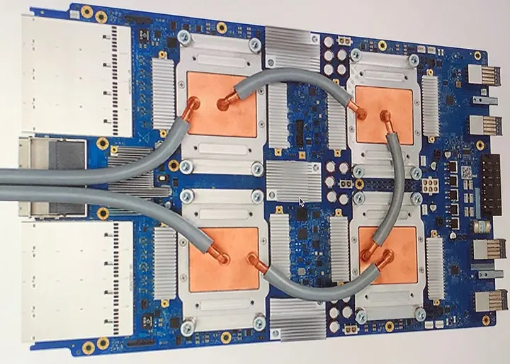
This development journey has progressed to reach the eighth generation in 2026. On April 22, 2026, Google announced the TPU 8t (training) and TPU 8i (inference) chips. The TPU 8t model features 12.6 FP4 PFLOPs of performance and 216 GB of HBM3e memory, which scales up to 9,600 chips via the Virgo network fabric to provide 121 FP4 ExaFLOPs of performance. On the other hand, the TPU 8i chip features 10.1 FP4 PFLOPs, 288 GB of HBM3e memory, and 384 MB of SRAM. Broadcom and TSMC have played a significant role in the production of all of Google's TPU models.
The importance of NPUs in consumer devices and edge computing
Beyond data centers, the use of NPUs is increasing widely in smartphones, laptops, and edge devices. In July 2018, Google announced the Edge TPU, which has the capacity to perform 4 trillion operations per second (4 TOPS) on 2 watts of power. It works on TensorFlow Lite and 8-bit calculations. Asus has utilized this technology in single-board computers such as the Tinker Edge T and Tinker Edge R.
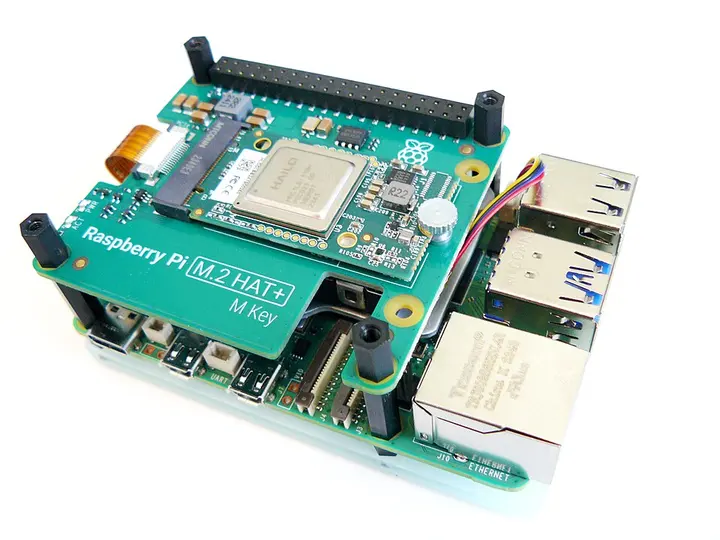
In consumer devices, Apple Silicon, Qualcomm, Samsung, Huawei, and Google Tensor processors have built-in NPUs. By using an NPU in graphics rendering, a scene rendered at 540p resolution (30 fps) can be upscaled in real-time to 2160p (240 fps), which reduces the power consumption of the main GPU. Intel's Meteor Lake processors include a VPU for vision processing.
The use of NPUs is also increasing in scientific computing. By using the Ozaki scheme, high-precision (FP64) calculations can be simulated on low-precision (FP16 or INT8) NPUs. This method has recorded a 6-fold increase in speed on Nvidia consumer GPUs. To simplify software development in this field, open standards such as OpenCL, Vulkan, and SPIR-V are being developed by the Khronos Group.