A Remarkable Microscope That 'Touches' the World of Atoms: Technology and Working Principle of Atomic Force Microscopy
Instead of light or lenses, the Atomic Force Microscope (AFM) uses an extremely fine probe to 'feel' surfaces, generating three-dimensional images down to the atomic level.

In the world of science, when we talk about atoms and molecules, even imagining seeing them seems difficult. Ordinary optical microscopes cannot see atoms due to the limitations of light waves. However, Atomic Force Microscopy (AFM) is a revolutionary technology that creates images by 'touching' the surface instead of using light. According to Wikipedia and news reports, the capability of this microscope is 1,000 times greater than an ordinary optical microscope, capable of showing details down to a small fraction of a nanometer.
The history of this technology is quite interesting. AFM was invented in 1985 by IBM scientists. For its predecessor instrument, the Scanning Tunneling Microscope (STM), Gerd Binnig and Heinrich Rohrer received the Nobel Prize in Physics in 1986. Subsequently, Binnig, Quate, and Gerber built the first experimental AFM in 1986. The first commercially available AFM arrived on the market in 1989, which changed the way materials are studied at the nanoscale.
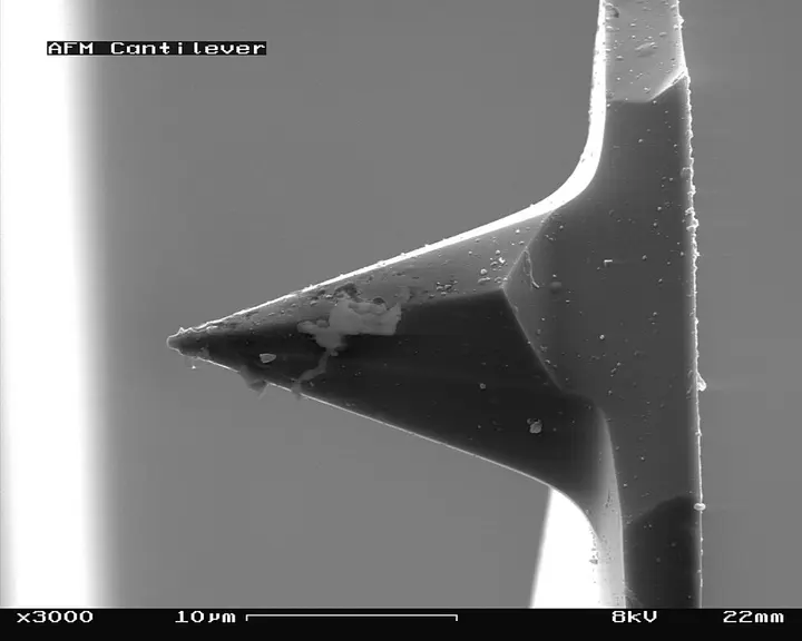
To understand the working mechanism of AFM, one can imagine a blind person's cane or the needle of an old-fashioned record player. This microscope has an extremely fine needle called a tip. This tip is attached to the end of a small flexible strip called a cantilever. When this tip comes very close to the surface of a sample, the cantilever bends due to the atomic forces between the tip and the surface. This deflection is so subtle that a laser beam is used to measure it.
- 1. Tip contactAn extremely fine needle-like tip goes very close to the sample surface.
- 2. Bending of the cantileverDue to atomic forces, a flexible strip called a cantilever experiences subtle bending.
- 3. Measurement by laserA laser beam is used to measure this subtle bending of the cantilever.
Key components and structure of AFM
The structure of an AFM includes several highly precise working parts. The most important part is the cantilever (1), which is held by a support (2). At the free end of this cantilever is a sharp tip (4), whose curvature diameter is on the order of nanometers. Piezoelectric elements (3) are used for scanning the surface. These are ceramic materials that can perform extremely subtle yet precise movements as soon as they receive an electrical signal.
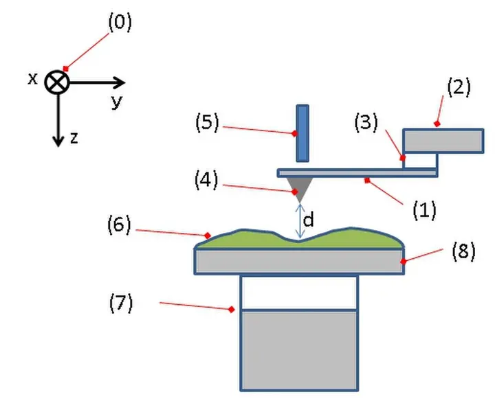

There is a sample stage (8) to hold the sample, which can move in all three directions with the help of an xyz drive (7). As the tip moves over the surface, the movement of the cantilever is recorded by a detector (5). Most AFMs use the laser deflection method. In this method, laser light strikes the back surface of the cantilever and falls onto a photodiode detector. If the cantilever bends even slightly, the position of the laser reflection changes, which accurately measures the change in the height of the needle.
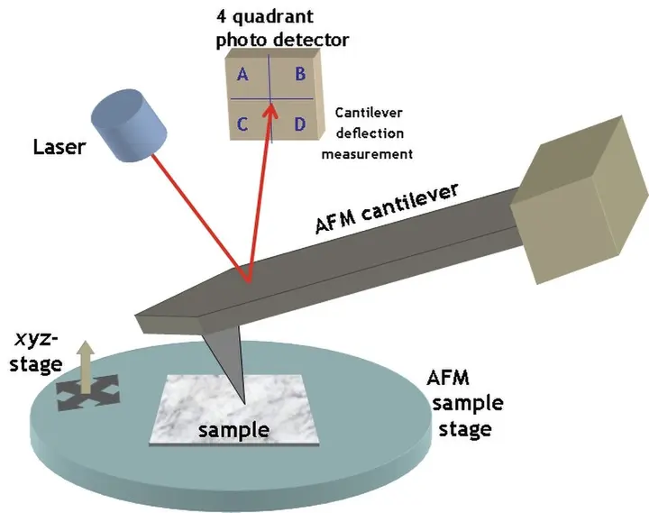
Image formation process and modes
AFM does not measure just a single point, but instead performs a raster scanning across the entire surface. That is, it moves across the surface line by line and collects height information at each point. This information is processed by a computer to generate a three-dimensional map of the surface, which is called topography. This map is generally represented as a pseudocolor plot, where different colors indicate different heights.
- Arrival of the tipThe extremely sharp tip is brought very close to the sample surface.
- Force responseThe cantilever bends due to attractive or repulsive forces between surface atoms and the tip.
- Laser trackingThe laser beam falling on the cantilever precisely records its deflection on the detector.
- Data processingThe computer converts these movements into digital signals to create a three-dimensional image of the surface.
AFM can operate primarily in three ways or 'modes'. The first is the contact mode, in which the tip continuously moves while touching the surface. The second is the tapping mode, in which the cantilever constantly experiences oscillation and gently 'taps' the surface. This mode is excellent for soft samples because it does not damage the surface. The third is the non-contact mode, in which the tip maintains a distance without touching the surface by using only forces such as van der Waals forces.
| Name of the mode | Working principle and use |
|---|---|
| Contact mode | The tip moves while constantly touching the surface. |
| Tapping mode | The cantilever constantly experiences oscillation and is excellent for soft samples. |
| Non-contact mode | The tip uses Van der Waals forces without touching the surface. |
Comparison with other microscopes
A major difference between AFM and other microscopes such as optical or electron microscopes (SEM) is that AFM uses no lenses or beam irradiation. Because of this, it is free from the limitations of light diffraction and aberration. SEM requires a vacuum to view samples and often necessitates a special coating on the sample. In comparison, AFM can operate in air or liquid media, which is highly advantageous for biological samples.
AFM is also unmatched in terms of resolution. In 1993, Ohnesorge and Binnig achieved atomic-level resolution in a liquid medium. Subsequently, true atomic resolution on a silicon 7x7 surface was demonstrated by Giessibl. Today, AFM is so powerful that it can even provide sub-atomic resolution, meaning the electron density structure within a single atom can also be observed.
Application and importance in various fields
AFM is used not only for viewing surfaces, but also for force measurement and manipulation. The strength or stiffness of a material can be measured through force spectroscopy. In manipulation, individual atoms can be moved using the tip, or extremely minute lithography can be performed on the surface. This capability makes it one of the most important tools of nanotechnology.
In biology, AFM is used to study protein complexes and microtubules. In cancer research, AFM is used to identify the difference in stiffness between normal cells and cancerous cells. Furthermore, in solid-state battery research, advanced methods like conductive AFM (C-AFM) are increasingly being used to understand local conductivity and the degradation process of batteries.
Formed by the combination of precision and science, this instrument gives us a glimpse into a world that has always been invisible to our naked eyes. Whether it is examining the arrangement of atoms or talking about creating new materials, AFM has become an indispensable tool in modern science laboratories.