Scanning Tunneling Microscope: The Remarkable Technology for Visualizing and Manipulating Atoms via Quantum Physics
An insightful look at how the unique phenomenon of quantum tunneling enables precise surface imaging of individual atoms, the fundamental building blocks of matter.
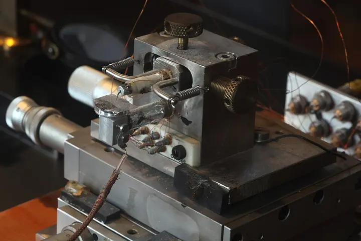
For centuries in human history, the fundamental particles of matter, namely atoms, could only be imagined through calculations and theories. However, this scenario changed completely in 1981 when the Scanning Tunneling Microscope (STM) was invented by two scientists working at IBM Zürich, Gerd Binnig and Heinrich Rohrer. While ordinary optical microscopes cannot see objects at the nanometer scale due to the limitations of light wavelength, the STM proved its ability to provide three-dimensional images of surfaces at the atomic level. For this epoch-making invention, both researchers were awarded the Nobel Prize in Physics in 1986.
The power of this microscope is so extraordinary that it can distinguish details smaller than 0.1 nanometers (nm), and its depth measurement capability is as precise as 0.01 nanometers, or 10 picometers (pm). Due to this incredible resolution, scientists can not only clearly see individual atoms arranged on a surface but can also move them at will to create new structures. Most STM devices are operated at extremely low temperatures near absolute zero and in ultra-high vacuum, although some special versions can also work in normal air, water, or at temperatures exceeding 1000 °C.
The Miracle of Quantum Tunneling
The entire operating principle of the Scanning Tunneling Microscope is based on a highly fascinating principle of quantum mechanics: quantum tunneling. According to classical physics, if a particle does not have sufficient kinetic energy, it cannot overcome an energy barrier, much like a ball cannot reach the other side of a hill if it lacks the energy to climb it. However, in quantum physics, an electron is not just a particle but also a wave, which can be explained by a wave function represented by the Schrödinger equation.
When an extremely sharp needle (tip) of a conductive material is brought very close to the surface of a sample and a small bias voltage is applied between them, electrons jump across the vacuum barrier between them by creating an invisible tunnel. The minute electric current that flows through this process is called the tunneling current, which is in the sub-nanoampere range. This tunneling current depends exponentially on the distance between the tip and the surface; if the distance changes by even the diameter of an atom, a large surge or drop in the electric current is recorded.
- Needle positioningAn extremely sharp metal needle is brought to an ultra-fine distance of 0.4 to 0.7 nanometers from the sample surface.
- Voltage and tunnelingElectrical voltage is applied between the needle and the sample, causing electrons to flow by crossing the vacuum barrier via quantum tunneling.
- Scanning and dataThe needle moves horizontally and vertically over the surface, and by measuring changes in the tunneling current, a three-dimensional image of the surface is prepared.
- 1. Coarse ApproachAn extremely thin conductive needle is brought very close to the sample surface via mechanical control.
- 2. Piezoelectric fine controlBy applying voltage to the piezoelectric tube, the needle is positioned at a precise distance of 4 to 7 Angstroms from the surface.
- 3. Bias voltage and tunnelingWhen voltage is applied, electrons flow from the vacuum towards the needle via quantum tunneling, creating a sub-nanoampere current.
- 4. Raster scanning and feedbackThe needle moves over the surface in the x-y direction, and the feedback system records changes in current or height.
- 5. Three-dimensional image generationThe computer combines data from each grid point to present an accurate atomic-level digital topographic image.
Scanning Mechanism and Piezoelectric System
In this device, the task of moving the needle over the surface is extremely delicate and precise. The distance between the needle and the sample is generally maintained at 4 to 7 angstroms (Å), which is 0.4 to 0.7 nanometers. This distance is such that an attractive force prevails between the two (between 3 and 10 Å), but if the distance becomes less than 3 Å, a repulsive force begins to act, posing a risk of the needle colliding with the surface and breaking.
To control the needle with precision at such delicate distances, a piezoelectric scanner tube is used. Piezoelectric materials are special substances that undergo contraction or expansion at the nanometer level in their shape or length when a voltage is applied to them. In an STM, a tube typically made of lead zirconate titanate ceramic is used, which has a piezoelectric coefficient of approximately 5 nanometers per volt. Four metal electrodes are attached to the outer surface of this tube to move the needle back and forth in the x and y directions, while the inner part controls it in height, i.e., the z direction.

Imaging Methods: Current and Height Mode
When a surface is scanned by an STM, a digital image is primarily prepared through two methods: constant-current mode and constant-height mode. In constant-current mode, feedback electronics continuously vary the z-direction piezoelectric voltage to maintain the tunneling current at a fixed value. If an atom rises on the surface, the current begins to increase, causing the feedback loop to lift the needle slightly. This mode is somewhat slow because the feedback must be adjusted at every point, but it is extremely safe for uneven surfaces and provides information on both surface topography and electron density.
On the other hand, in constant-height mode, the z-height of the needle is kept stable and it is moved rapidly horizontally and vertically across the surface. A map is prepared by directly measuring the rapid changes in tunneling current that occur according to the surface's pits and peaks. This mode is much faster, but there is a significant risk of the needle colliding if a large atom or high peak is suddenly encountered on the surface. The entire scanning process takes place in a grid of 128×128 to 1024×1024 or more points, so the raw image produced is black and white (grayscale), and color is added later only for analysis.
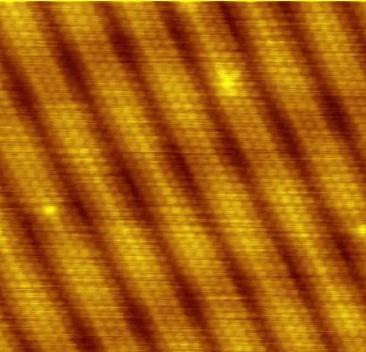
The actual images of surfaces obtained with the help of this method display regular arrays of atoms. It was through this technology that the remarkable view of the arrangement of atoms on crystalline metals, such as the surface of gold, became possible for the first time.
| Criteria | Constant-current mode | Constant-height mode |
|---|---|---|
| Tunneling current | Kept stable by feedback | Changes continuously according to location |
| Needle height (z) | Changes continuously according to surface | Remains constant during full scan |
| Scanning speed | Slow (due to feedback loop) | Very fast |
| Risk of needle collision | Extremely low and safe | Higher risk on rough surfaces |
| Data type | Topography and charge density | Direct change in tunneling current |
Spectroscopy and Atomic Manipulation
Merely observing the shape of a surface is not the only capability of STM. In an advanced method called Scanning Tunneling Spectroscopy (STS), the tip is held stationary directly above a specific atom or impurity, and the current is measured while varying the voltage. Through this process, the Local Density of States (LDOS)—that is, the availability of electrons at various energy levels in the sample—can be determined, which has proven revolutionary in understanding the electronic properties of materials at the quantum level.
Furthermore, the STM tip can be used like a tiny tweezer to move individual atoms or molecules on a surface. When the tip is brought extremely close to an atom and a high voltage is applied, it can attract the atom and place it at a desired location. Scientists have demonstrated the immense potential of nanotechnology by arranging molecules such as carbon monoxide on surfaces to create various logos and letters.
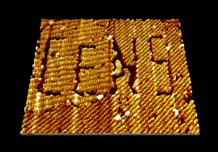
STM has also proven highly useful in understanding how atoms of various metals aggregate on surfaces and form structures. For example, the formation of nanoscale islands of silver atoms on a surface can be clearly observed using this instrument.

Mechanical Challenges and Specialized Research
Operating Scanning Tunneling Microscopy successfully is a major engineering challenge, as vibrations from fans running in a building or vehicles passing on the road outside can cause the tip to collide with the surface. Therefore, excellent vibration isolation is essential. Binnig and Rohrer used magnetic levitation in their first instrument, whereas today's modern instruments utilize mechanical springs, gas springs, and eddy-current damping.
For highly sensitive experiments, these microscopes are placed in special concrete anechoic chambers that are free from noise and electromagnetic waves. To create the tip, tungsten or platinum-iridium wire is used, which is sharpened at the end via electrochemical etching until only a single atom remains at the tip. Today's advanced high-speed video-rate STM devices are capable of live recording of chemical processes and atomic diffusion occurring on surfaces at a frame rate of 80 Hz.