The Digital Eye Revolution: The Science Behind Smartphone Cameras and the Mechanism of CMOS Sensors
An in-depth exploration of the architecture, working principles, and triumph over CCD technology of the CMOS image sensor, considered the heart of modern smartphones and digital cameras.
The Heart of the Camera Revolution: What is CMOS Technology?
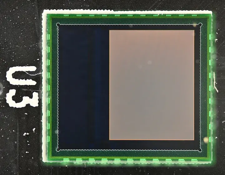
The crisp photographs we capture in a split second from our smartphones, the selfies we share on social media, or the high-definition videos we record all rely on a small yet extremely powerful silicon chip working behind the scenes. This chip is known as the CMOS Image Sensor (Complementary Metal-Oxide-Semiconductor Image Sensor). In simple terms, a CMOS sensor is the "artificial eye" of a digital camera, capturing the photon particles of light coming through the lens and converting them into an electronic digital image.
Every image sensor contains millions or billions of tiny cells, which we call pixels (the smallest unit of an image). In modern CMOS sensors, each pixel measures light by itself, converts it into an electrical current, and amplifies the signal right there on the spot. This principle is called an Active-Pixel Sensor (APS). It is precisely because of this technology that today's cameras have become extremely small in size, consume very little power, and possess remarkable light-gathering capabilities.

From CCD to CMOS: The History of Digital Photography
The beginning of digital imaging took place in 1969 at Bell Laboratories with the invention of the Charge-Coupled Device (CCD) by Willard Boyle and George E. Smith. CCD sensors ruled the camera industry for a long time. However, a major limitation of CCDs was that the charge of all pixels had to be read out sequentially by passing it through a single corner of the chip. Since this charge transfer process could tolerate no error whatsoever, CCD sensors consumed a substantial amount of electricity, caused the chip to heat up, and had an extremely complex manufacturing process.
In the 1960s, Peter Noble and G. Weckler introduced the concept of the Passive-Pixel Sensor (PPS), but due to the lack of amplification, it produced excessive electronic noise (blur or interference). In 1967, Peter Noble introduced the concept of the 'active pixel' by placing transistors inside each pixel. Subsequently, in 1985, a team led by Tsutomu Nakamura of the Olympus company created the first micron-level MOS (Metal-Oxide-Semiconductor) active-pixel sensor based on the Charge Modulation Device (CMD) and coined the term 'Active-Pixel Sensor' (APS).

But the real revolution came when Nobukazu Teranishi and his team at NEC invented the 'Pinned Photodiode' (PPD) in 1980. This innovation was named the pinned photodiode in 1984 by B.C. Burkey of the Kodak company. Due to the PPD, lag in the image, dark current (noise in the dark), and electron leakage were completely reduced. In 1992, the successful development of the CMOS active-pixel sensor took place at Mitsubishi Electric, and in 1993 at NASA's Jet Propulsion Laboratory (JPL), which laid the foundation for today's modern cameras.
Architecture and Working Mechanism of CMOS Sensors
The pixel of a modern CMOS sensor primarily operates on a 4T (four-transistor) architecture. Inside it, there are a pinned photodiode (PPD), a Floating Diffusion node (FD), and four microscopic transistors. Let us understand how this system converts a single ray of light into digital data.
First, when the camera shutter opens, photons of light fall on the pinned photodiode. Through the photoelectric effect, the photons release electrons from the silicon atoms. These electrons accumulate in the photodiode. Then the transfer gate (TG) turns on, and this accumulated charge is transferred to a tiny capacitor called floating diffusion (FD). PPD technology helps complete this process without losing any data.
- 1. Photon Absorption (PPD)Photons of light coming through the lens release electrons into the pinned photodiode.
- 2. Charge Transfer (TG)When the transfer gate turns on, the charge is transferred to the floating diffusion (FD) node.
- 3. Voltage Amplification (SF)The source follower transistor converts the charge into voltage and amplifies the signal.
- 4. Digital Conversion (ADC)Column ADC converts the analog voltage signal into digital data of 0s and 1s.
Next, this charge is converted into a voltage signal and amplified by the source follower (SF) transistor. The select transistor (SEL) connects this pixel to the processing line, and the reset transistor (RST), after the work is done, empties the FD node and prepares it for the next frame. In this way, each pixel sends its voltage signal to the analog-to-digital converter (ADC) located at the edge of the chip, where it is converted into digital codes of 0s and 1s.
Important Statistics, Milestones, and Market Domination
In its first two decades, CMOS sensor technology rendered CCD technology almost obsolete in the market. In the early 2000s, CMOS was used only in cheap webcams and security cameras because CCD had better color and image quality. But in the 2000s, specifically in 1999, an 800x600 color CMOS sensor was manufactured by Hyundai Electronics in a 0.5 um DRAM process, which featured integrated ADCs and 4T PPD.
In 2007, Sony developed a separate analog-to-digital converter circuit for each column (Column ADC), which multiplied the readout speed manifold and significantly reduced noise. Due to this success, the market share of CMOS sensors grew rapidly.
By 2007, CMOS's share of the global image sensor market reached 54%, surpassing CCD for the first time. By 2012, this share had grown to 74%, and in 2017, CMOS established a near-monopoly, capturing 89% of worldwide image sensor sales. Sony, OmniVision, Samsung, and silicon foundries invested billions of dollars in this sector.
| Year | Technology / Discovery | Institution / Researcher |
|---|---|---|
| 1969 | Invention of CCD sensor | Willard Boyle and George Smith (Bell Labs) |
| 1967 | Active Pixel Concept (APS) | Peter Noble |
| 1980 | Pinned Photodiode (PPD) | Teranishi, Shiraki, Ishihara (NEC) |
| 1985 | First MOS Active-Pixel Sensor | Tsutomu Nakamura Team (Olympus) |
| 1993 | CMOS Active-Pixel Sensor | NASA JPL / Mitsubishi |
| 2009 | Back-Illuminated (BSI) CMOS | Sony Commercialization |
Back-Illuminated and Stacked Sensors: The Power of Modern Cameras
In traditional front-illuminated CMOS sensors, layers of metal wiring and transistors were positioned on top of the silicon. Because of this, nearly 30% to 40% of the light coming through the lens would collide with these wires and go to waste, resulting in poor photography at night or in low-light conditions.
In 2009, Sony commercially introduced the back-illuminated (BI or BSI) CMOS sensor. In this new design, the silicon wafer was thinned and inverted, moving the metal wiring behind the sensor so that the photodiodes came into direct contact with light. BSI technology doubled (2x) the light sensitivity of the sensor.
[[fig 1_alt]]
Subsequently, in 2012, Sony launched the "Stacked CMOS Sensor." In this design, the pixel array (the upper section of silicon) and the logic processing circuit (the lower section) were built as two separate layers and bonded together. This made it possible to obtain a very large pixel area even within a small smartphone sensor, while dramatically increasing processing speed.
Smartphones, India, and the Future of Quanta Imaging
Today, it has become possible to fit sensors resembling those of large DSLRs into smartphones. Although there is a huge size difference between the sensor of a large full-frame camera like the Canon EOS 5D Mark IV and a tiny smartphone sensor, smartphone cameras deliver unimaginable quality thanks to software, BSI architecture, and computational photography. In 2014, Phase One launched a medium-format digital back utilizing a Sony sensor, effectively putting an end to CCDs in professional photography as well.
In a country like India, ground-level applications such as social media, digital content creation, Aadhaar biometric authentication, and smart city CCTV frameworks depend entirely on the low-cost production and high efficiency of CMOS sensors. In the medical field, from lensless imaging of blood cells to LiDAR and camera vision in autonomous cars, CMOS sensors have become indispensable.
The next revolution in imaging science is now arriving in the form of the "Quanta Image Sensor" (QIS). The objective of QIS is to count single photons of light one by one. It will feature billions of sub-micron-sized photoelements called "jots" on the sensor, which will perform bit-plane readouts hundreds or thousands of times per second and generate terabits of data per second (Terabits/sec). This digital eye of the future will permanently erase the word "darkness" from the camera's vocabulary.