Hall Effect Sensors: Operating Modern Devices Through the Synergy of Magnetic Fields and Electric Current
Discovered by Edwin Hall in 1879, this physical phenomenon has today become the foundational technology providing precise control and sensing in everything from smartphones to automobiles.
The Convergence of Invisible Magnetic Force and Electricity
Among the sensors that we do not see in modern electronic devices and autonomous vehicles but that remain constantly active, the Hall effect sensor is one of the most important. Whether one needs to measure the speed of a vehicle, know the precise rotation of an engine's crankshaft, or automatically turn off a laptop screen as soon as its lid is closed, it is not possible without this tiny construction. Built on a fundamental principle of physics, this sensor generates electrical signals by detecting the presence of a magnetic field without any direct mechanical contact.

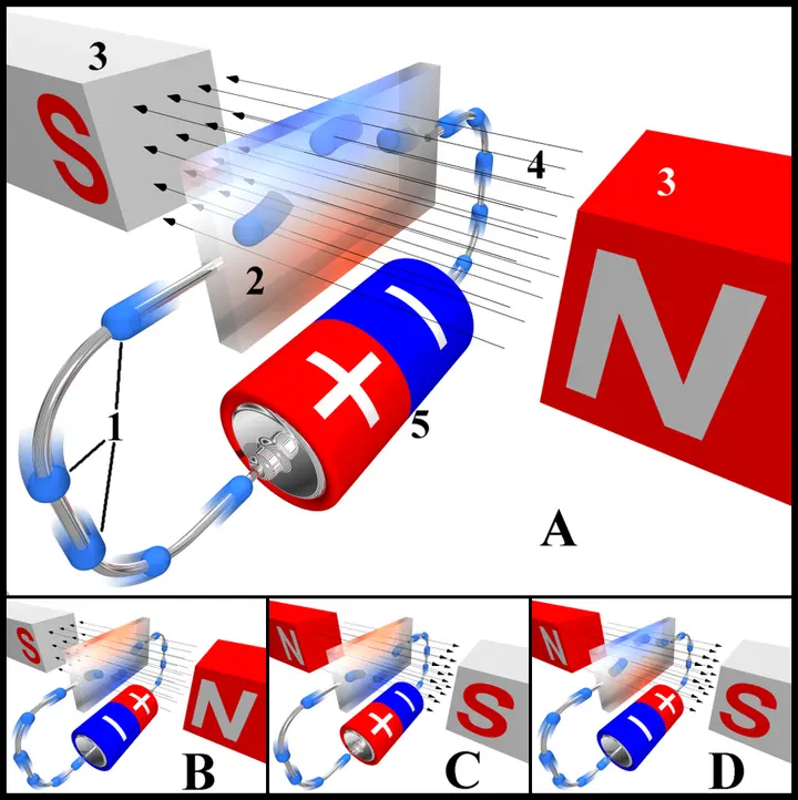
Behind this entire process lies a physical phenomenon named the Hall effect. When an electric current flows through an electrical conductor and a magnetic field is applied perpendicularly to it, a orthogonal voltage difference is generated between the two sides of that conductor. This specific electrical pressure is called the Hall voltage.
Historical Background and Edwin Hall's Discovery
The historical beginning of this phenomenon took place in the first half of the nineteenth century. In the 1820s, André-Marie Ampère observed that a mechanical force acts on a conductor wire situated in a magnetic field. Subsequently, in the period 1861-1862, James Clerk Maxwell laid a strong mathematical foundation for electromagnetism in his research paper 'On Physical Lines of Force'.
While studying Maxwell's principles, a question arose in the mind of the American physicist Edwin Hall. He wanted to know whether the magnetic field exerts a force directly on the conductive material or on the electric current flowing inside it? If this force acted only on the flowing current, it should push the current toward one side of the conductor, resulting in a measurable small voltage.
- Conduction of electric currentElectrons or other charge carriers move in a regular direction through a conductive material.
- Effect of magnetic fieldLorentz force is applied to moving particles when a perpendicular magnetic field is added.
- Displacement of particlesUnder the influence of force, instead of going straight, particles deflect and accumulate towards one surface of the conductor.
- Generation of electric fieldAn internal electric field is created due to the separation of positive and negative charges on opposite surfaces.
- Constant Hall voltageA stable voltage difference is established when the Lorentz force and electric force are balanced.
In the year 1879, while working on his doctoral degree at Johns Hopkins University in Baltimore, Maryland, Edwin Hall experimentally demonstrated and measured this voltage. This experiment, conducted eighteen years before the discovery of the electron, was extremely remarkable. He published this research under the title 'On a New Action of the Magnet on Electric Currents'.

How This Principle Works: Lorentz Force and Charge Separation
Electric current in any conductor wire is actually the flow of countless small charge carriers such as electrons, holes, or ions. When no external magnetic field is present, these particles generally move in a straight path while colliding with impurities or phonons.
However, when a magnetic field is applied perpendicularly to the conductor, a Lorentz force acts on the moving particles. The formula for this force is equal to the product of the electric charge, the velocity of the particles, and the magnetic field. Due to this force, instead of moving straight, the particles take a turn and begin to accumulate toward one edge of the conductor.
The accumulation of a negative charge on one side exposes a positive charge on the opposite surface. This uneven distribution of electric charge creates an internal electric field that opposes the Lorentz force. In the state of equilibrium, these two forces cancel each other out, and a stable Hall voltage is maintained as long as the current continues to flow.
| Symbol | Dimension / Physical quantity | Effect |
|---|---|---|
| VH | Hall voltage | Resultant electrical pressure |
| RH | Hall coefficient | Depends on material and carrier density |
| Ix | Electric current | Voltage increases as current increases |
| Bz | Magnetic field | Voltage increases as the field becomes stronger |
| d | Thickness of the conductor | Voltage increases if thickness is less |
Calculation and Material Properties
The mathematical value of the Hall voltage is obtained by multiplying the Hall coefficient of the conductor, the electrical current flowing through it, and the magnetic field, and dividing by the thickness of the conductor. This Hall coefficient is a specific property of the material, which depends on the number, type, and density of the particles constituting the electric current.
The width of the conductor is automatically eliminated from this equation, so that the smaller the thickness of the conductor, the more distinct the Hall voltage obtained. This is the exact reason why extremely thin strips or wafers are used in laboratories and sensor manufacturing.
Interestingly, whether the electric charge is positive or negative, the Lorentz force deflects them in the same direction. However, the polarity of the generated voltage is reversed. It is due to this characteristic that the scientific world obtained concrete proof for the first time that electrical current in most metals flows through mobile electrons rather than protons.

Importance in Modern Devices and Semiconductors
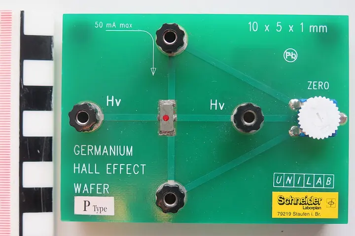
Since the density of free electrons in pure metals is very high, the Hall coefficient remains low, and consequently, the resulting voltage is also very small. However, in semiconductor materials such as silicon and germanium, because the number of charge carriers is limited, a comparatively much larger Hall voltage can be obtained. N-doped or P-doped germanium wafers demonstrate this principle with extreme accuracy.
Modern sensors based on this principle play a leading role today in robotics, mobile gadgets, and industrial control systems. Since there is no mechanical wear and tear, these sensors provide accurate results for years even amidst dust, moisture, or vibration, which is highly essential in today's digital age.