Silicon Photonics: The Data Transmission Revolution from Copper Wires to the Speed of Light
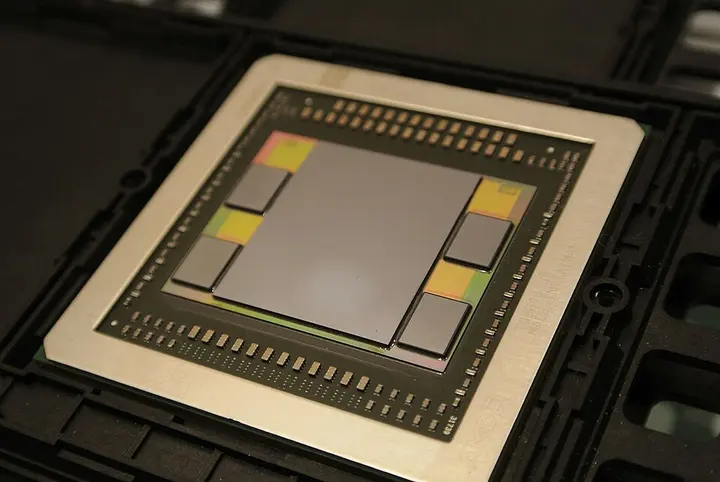
Silicon photonics technology, which transfers data using light rays instead of electricity in computer chips, is creating a new revolution in the semiconductor sector.

Today, the demand for digital data is growing at a compound rate. Copper wires have traditionally been used to exchange information inside and between computer processors. However, as processing speeds increase, the electric current flowing through copper wires generates more heat and energy waste, becoming a major obstacle to advancing Moore's Law. As a solution to this problem, Silicon Photonics technology has emerged, which uses optical rays, or light, instead of electrons to transmit information.
Silicon Photonics is a technology in which silicon is used as an optical medium. Microscopic photonic components are prepared by carving this silicon structure with sub-micrometre level precision. Typically, this system operates at an infrared wavelength of 1.55 micrometres, which is widely used in fiber optic telecommunications. In this chip, the silicon is generally situated on a layer of silica, which is called Silicon on Insulator (SOI).
The biggest feature of this technology is that it utilizes existing semiconductor fabrication technology. Since silicon is already the foundation of most integrated circuits, it has become possible to combine optical and electronic components onto a single microchip to create a hybrid device. In 2006, Intel's then Senior Vice President Pat Gelsinger said, "Today optics is a niche technology, but tomorrow it will become the mainstream of every chip we build." Major semiconductor companies like IBM and Intel are conducting heavy research in this field.
From Modulation to Detection: How This System Works
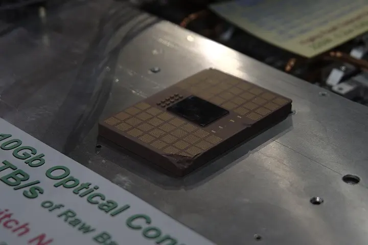
To transmit information in an optical connection, data must first be converted from the electrical domain to the optical, or light, domain. This task is done by an electro-optic modulator or a directly modulated laser. The modulator encodes the data by changing the intensity or the phase of the light. In silicon photonics, modulation is achieved by varying the density of free charge carriers.
Changes in the density of electrons and holes bring about variations in the real and imaginary parts of silicon's refractive index, which are expressed by Soref and Bennett empirical equations. These modulators can be forward-biased PIN diodes, which provide a large phase shift but are slow in speed, or reverse-biased p–n junctions. Besides this, non-resonant modulators such as Mach-Zehnder interferometers (MZIs) are millimeters in size and used in telecoms, whereas resonant devices such as ring-resonators are only tens of micrometers in size.
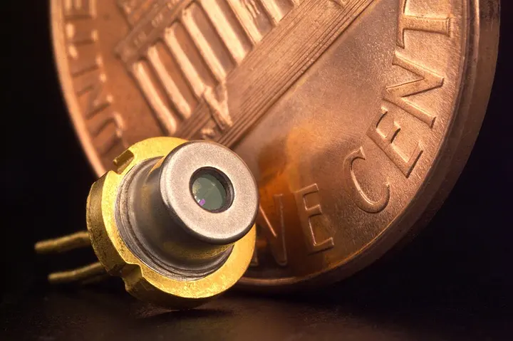
On the receiver side, the optical signal is converted back into electrical data by a semiconductor photodetector. Pure germanium is most commonly used for this because its band-gap is smaller than the photon energy. Researchers have also fabricated silicon-germanium avalanche photodiodes capable of operating at a speed of 40 Gbit/s. Apart from that, graphene photodetectors also possess the potential to deliver higher bandwidth and lower energy consumption than germanium.
Gbit/s
- 1. Electro-optic modulationElectrical signal is converted into light waves by an electro-optic modulator or laser.
- 2. Silicon waveguide propagationLight rays advance with sub-micrometer precision through a silicon-on-insulator (SOI) waveguide.
- 3. Optical signal routingPhase and intensity of light are controlled using a Mach-Zehnder interferometer or ring-resonator.
- 4. De-signaling via photodetectorGermanium-based photodetector converts the optical signal back into electrical data.
Speed and Performance Figures: From Laboratory to Reality
Astonishing progress has been recorded in silicon photonics technology over the past decade and a half. In 2010, Intel successfully demonstrated a 50 Gbit/s optical connection using silicon photonics. Subsequently, in December 2015, the first microprocessor with optical input/output (I/O) was demonstrated using a "zero-change" CMOS photonics approach, which is called fiber-to-the-processor. This device was based on the 45 nm SOI node and its bi-directional chip-to-chip link ran at a speed of 2×2.5 Gbit/s, with a total energy consumption of just 16 pJ/b (picojoules per bit).
In the realm of manufacturing and scaling, IBM announced in 2012 that they had achieved optical components at a 90 nanometer (90 nm) scale that can be integrated with standard chip fabrication techniques. In September 2013, Intel announced a technology to transmit data at a speed of 100 Gbit/s over a cable with a diameter of just 5 millimeters to connect data center servers. For comparison, traditional PCI-E data cables offer a speed of 8 Gbit/s, networking cables 40 Gbit/s, and the new version of USB 10 Gbit/s.
This technology has also demonstrated its strength in long-distance telecommunications. Researchers from Sandia, Kotura, NTT, Fujitsu, and various academic institutions successfully operated a prototype to transmit data at a speed of 12.5 Gbit/s over a distance of 80 kilometers (80 km) using microring silicon devices.
| Year / Organization | Based Technology | Data Transfer Speed | Features / Energy Consumption |
|---|---|---|---|
| 2010 (Intel) | Silicon Photonics Connection | 50 Gbit/s | Initial optical connection prototype |
| 2012 (IBM) | 90 nm scale components | Standard chip scale | Compatible with conventional chip manufacturing methods |
| 2015 (Zero-change CMOS) | 45 nm SOI node | 2 × 2.5 Gbit/s | 16 pJ/b energy consumption, fiber-to-the-processor |
| 2010 (Sandia/NTT/Fujitsu) | Microring silicon device | 12.5 Gbit/s | Long-distance transmission up to 80 km |
Nonlinear Optics and On-Chip Laser Challenges
When light passes through silicon devices, certain non-linear optical phenomena are observed. Among these, the Kerr effect, Raman effect, two-photon absorption, and the interaction between free charge carriers are primary. Due to these non-linear properties, light itself can interact with light, facilitating tasks such as all-optical signal routing and wavelength conversion. It also supports unique phenomena like soliton propagation.
A major debate in optical computing is on-chip lasers versus off-chip lasers. Some researchers believe the laser source should be on the chip itself, while others advise keeping it external due to thermal (heat) issues. Computer chips heat up, and as the temperature rises, the quantum efficiency of the laser decreases. As a solution to this, hybrid silicon lasers have been developed, in which silicon is combined with other semiconductors such as Indium Phosphide. Apart from that, all-silicon Raman and Brillouin lasers have also been developed.
Optical routers have also been created using all-optical switching of optical signals. In 2013, the California and Israel-based startup company Compass-EOS introduced the world's first commercial silicon-two-photonics router.
AI Inference, 3D Integration, and Future Directions
Silicon photonics is also bringing a revolution in the field of Artificial Intelligence (AI), which is considered a new horizon of computing. Compared to processors with traditional transistors, optical AI inference processors consume extremely low energy. For this, Mach-Zehnder Interferometers (MZIs) are combined with nanoelectromechanical systems to make fractional changes in the phase of light.
To overcome space limitations on the chip, Monolithic Multilayer Photonic Integration (MPI) is used. Since the size of optical waveguides is hundreds of nanometers, which is much larger than the size of transistors, occupying space on expensive contemporary CMOS nodes is not economically viable. Through 3D integration, optical components are arranged in vertically stacked layers on a single chip. At UCLA, Bahram Jalali and his students developed Simox 3D Sculpting technology, through which optical circuits can be built up to 3 vertically coupled layers.
This technology is expanding from connections between GPU clusters in data centers to augmented reality (AR) displays. For instance, in 2015, the American startup Magic Leap announced that it was working on a silicon photonics-based light-field chip for AR displays. As the demand for data processing grows in the fields of AI and supercomputing, silicon photonics will replace traditional electronics and ensure the dawn of the optical era.